LC1463
300mA High PSRR, Fast Response Linear Regulator
DESCRIPTION
FEATURES
LC1463 series is a group of positive voltage
output, low power consumption, low dropout
voltage regulator.
LC1463 can provide output value in the range of
1.0V~4.5V every 0.1V step. It also can be
customized on command.
LC1463 includes high accuracy voltage reference,
error amplifier, current limit circuit and output
driver module with discharge capability.
LC1463 has excellent load and line transient
response and good temperature characteristics,
which can assure the stability of chip and power
system. And it uses trimming technique to
guarantee output voltage accuracy within ±2%.
Low Power Consumption: 35uA(Typ.)
Low output noise (47uVRMS)
Standby Mode: 0.1uA
Low dropout Voltage: 300mV@300mA (Typ.)
High Ripple Rejection: 70dB@10KHz (Typ.)
Low Temperature Coefficient: ±100ppm/C
Excellent Line regulation: 0.05%/V
Build-in chip enable and discharge circuit
Output Voltage Range: 1.0V~4.5V
(customized on command every 0.1V step)
Highly Accurate: ±2%
Output Current Limit
APPLICATIONS
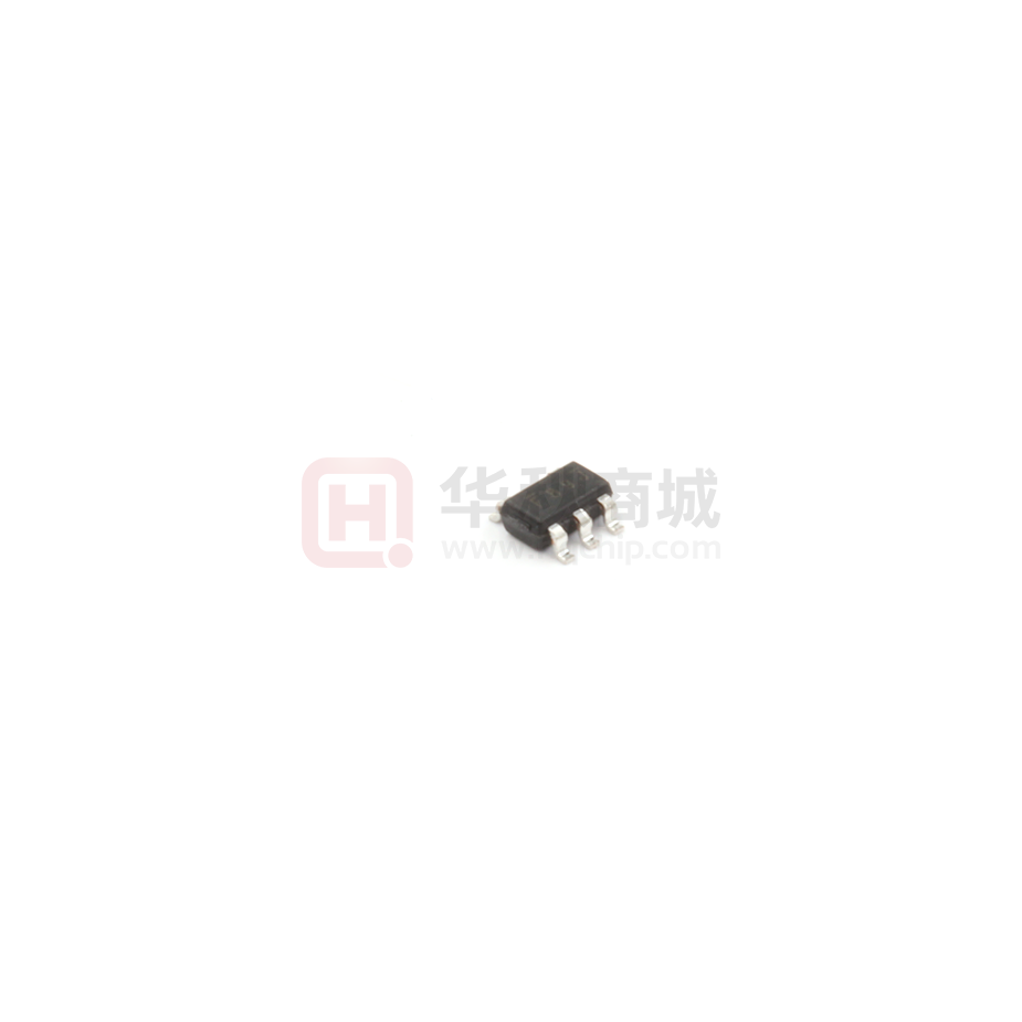
LC1463 is available in SOT-23-3, SOT23-5, SC-70-5
and DFN1x1-4 packages which are lead free.
Power source for cellular phones and various
kind of PCSs
Battery Powered equipment
Power Management of MP3, PDA, DSC,
Mouse, PS2 Games
Reference Voltage Source
Regulation after Switching Power
TYPICAL APPLICATION
ELECTRICAL CHARACTERISTICS
Input
VDD
Cin
CE
VOUT
LC1463
Output
Cout
GND
On/Off
NOTE: Input capacitor (Cin=1uF) and Output capacitor
(Cout=1uF) are recommended in all application circuit.
www.leadchip.com.cn
1
Your final power solution
�LC1463
ORDERING INFORMATION
LC1463 □
1□
2□
3□
4
Code
PIN CONFIGURATION
Description
Product Classification
Temperature&Rohs:
C:-40~85C ,Pb Free Rohs Std.
A: short circuit current >100mA
Package type:
A5:SC-70-5
B5A:SOT-23-5(A)
B5B:SOT-23-5(B)
B3: SOT23-3
KE:DFN1x1-4
Packing type:
TR:Tape&Reel (Standard)
Output voltage:
e.g. 15=1.5V
18=1.8V
45=4.5V
1
□
2
□
3
□
4
□
LC1463CA5TR□□
F : Product Code
X: Output Voltage
ZZ: Date Code
Product Classification
LC1463CB5ATR□□
F : Product Code
X: Output Voltage
ZZ: Date Code
Product Classification
LC1463CB5BTR□□
F : Product Code
MARKING DESCRIPTON
X: Output Voltage
ZZ: Date Code
F : Product Code
I: B type
X: Output Voltage
Product Classification
Vout
Code
Vout
Code
Vout
Code
1.0V
0
2.3V
3
3.6V
6
1.1V
1
2.4V
4
3.7V
7
1.2V
2
2.5V
5
3.8V
8
1.3V
3
2.6V
6
3.9V
9
ZZ: Date Code
1.4V
4
2.7V
7
4.0V
0
Product Classification
1.5V
5
2.8V
8
4.1V
1
1.6V
6
2.9V
9
4.2V
2
1.7V
7
3.0V
0
4.3V
3
1.8V
8
3.1V
1
4.4V
4
1.9V
9
3.2V
2
4.5V
5
2.0V
0
3.3V
3
2.1V
1
3.4V
4
2.2V
2
3.5V
5
F: Product Code
X: Output Voltage
LC1463CKETR□□
XX: Output Voltage
Vss
Vin
Vout
CE
NC
Z: The Year of manufacturing,”1” stands for year
2011,”2” stands for year 2012,and “8” stands for year
2018.
Z: The week of manufacturing. ”A” stands for week
1,”Z” stands for week 26,” A ” stands for week 27,” Z ”
stands for week 52.
www.leadchip.com.cn
LC1463CB3TR□□
2
Ground Pin
Supply Voltage Input
Output Voltage
Chip Enable
No Connection
Your final power solution
�LC1463
ABSOLUTE MAXIMUM RATING
Parameter
Value
Max Input Voltage
Operating Junction Temperature(Tj)
Output Current
Ambient Temperature(Ta)
Package Thermal Resistance (jA)
Power Dissipation
8V
125C
300mA
-40C –85C
220C / W
220C / W
250mW
250mW
250mW
600mW
-40C -150C
260C,10S
SOT-23-5
SOT-23-3
SC70-5
SOT-23-5
SOT-23-3
DFN1x1-4
Storage Temperature(Ts)
Lead Temperature & Time
Note:
1) Heat Sink Area of PCB for DFN1x1-4 is recommended at least 2.5mmx4mm.
2) Package Thermal Resistance value can be affected by PCB design, outside radiator, ambient airflow, operating
power, it just shows for reference.
3) Exceed these limits to damage to the device.
4) Exposure to absolute maximum rating conditions may affect device reliability.
RECOMMENDED WORK CONDITIONS
Item
Min
Input Voltage Range
Ambient Temperature
Recommended
2
-40
Max.
Unit
6
85
V
C
ELECTRICAL CHARACTERISTICS
(Test Conditions: Cin=1uF,Cout=1uF,TA=25C, unless otherwise specified. )
LC1463, For Arbitrary Output Voltage
Symbol
Parameter
Vin
Input Voltage
Output
Voltage
Vout
Iout (Max.)
Vdrop
1
VOUT>1.5V
VOUT
很抱歉,暂时无法提供与“LC1463CB5ATR18”相匹配的价格&库存,您可以联系我们找货
免费人工找货- 国内价格
- 5+0.43962
- 20+0.40083
- 100+0.36204
- 500+0.32325
- 1000+0.30515
- 2000+0.29222
