JSM200N06C
60V N-Channel MOSFET
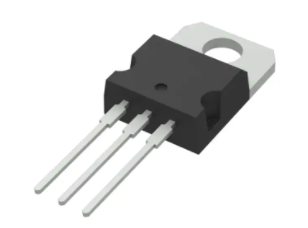
TO-220
60V N-Channel MOSFET
Features:
Low Intrinsic Capacitances.
MI
JS
Excellent Switching Characteristics.
Extended Safe Operating Area.
Unrivalled Gate Charge :Qg= 130nC (Typ.).
1.Gate
BVDSS=60V,ID=200A
2.Drain (D)
RDS(on) : 3.4mΩ (Max) @VG=10V
3.Source (S)
O
CR
□
□
□
□
□
□
□
(G)
100% Avalanche Tested
mi
Se
Absolute Maximum Ratings (TA=25°C unless otherwise noted)
Parameter
Symbol
ID3
PD
Unit
60
±20
180
116
720
28
870
1.96
245
-55~150
V
V
TC=25°C
TC=100°C
TC=25°C
Continuous Drain Current
Pulsed Drain Current
Avalanche Current
Avalanche energy
Maximum Power Dissipation
TC=25°C
TC=100°C
Junction & Storage Temperature Range
r
to
TJ, TSTG
Maximum
uc
IDP4
IAS5
EAS5
Drain-to-Source Voltage
Gate-to-Source Voltage
nd
co
VDSS
VGSS
A
mJ
W
°C
Thermal Characteristics
Symbol
Rθjc
Rθja
Parameter
Thermal Resistance-Junction to Case
Thermal Resistance-Junction to Ambient
www.jsmsemi.com
Typical
Unit
0.51
62.5
℃/W
第1/6页
�JSM200N06C
60V N-Channel MOSFET
Symbol
Static Characteristics
(TA=25°C unless otherwise noted)
Parameter
Test Conditions Min.
BVDSS
Drain-Source Breakdown Voltage
IDSS
Zero Gate Voltage Drain Current
VGS(th)
Gate Threshold Voltage
IGSS
Gate Leakage Current
RDS(on)1
Drain-Source On-Resistance
VSD1
I S3
trr
Qrr
MI
JS
RG
Gate Resistance
Max. Unit
VGS=0V,ID=250uA
VDS=60V,VGS=0V
TJ=100°C
VDS=VGS,ID=250uA
60
—
—
2
—
—
—
—
—
1
100
4
VGS=±25V, VDS=0V
VGS=10V, ID=70A
—
—
—
—
2.6
—
±100
3.4
—
ISD70A,V
—
—
—
—
—
—
48
69.6
140
—
—
V
A
nS
nC
—
9.0
—
Ω
—
—
—
—
—
—
—
4882
635
342
37.9
22.7
68.8
23.5
—
—
—
—
—
—
—
—
—
—
86.2
23.6
29.4
—
Diode Characteristics
Diode Forward Voltage
Diode Continuous Forward Current
Reverse Recovery Time
Reverse Recovery Charge
Typ
GS=0V
IF=70A,VDD=50V
dI/dt=100A/us
1.3
V
uA
V
nA
mΩ
O
CR
Dynamic Characteristics2
VGS=0V, VDS=25V
Frequency=1MHz
mi
Se
Ciss
Input Capacitance
Coss
Output Capacitance
Crss
Reverse Transfer Capacitance
td(on)
Turn-On Delay Time
tr
Rise Time
td(off)
Turn-Off Delay Time
Fall Time
tf
Gate Charge Characteristics2
Qg
Total Gate Charge
Qgs
Gate-to-Source Charge
Qgd
Gate-to-Drain Charge
VGS=0V, VDS=0V,
Frequency=1MHz
VDD=30V,ID=90A,
VGS=10V,RG=6Ω
nd
co
VDS=48V,VGS=10V
ID=90A
—
—
pF
nS
nC
r
to
uc
Note: 1: Pulse test; pulse width ≦ 300us, duty cycle ≦ 2%.
2: Guaranteed by design, not subject to production testing.
3: Package limitation current is 58 A.Calculated continuous current based on maximum allowable junction temperature.
4: Repetitive rating, pulse width limited by max junction temperature.
5: Starting TJ = 25°C,L = 0.5mH
www.jsmsemi.com
第2/6页
�JSM200N06C
60V N-Channel MOSFET
Typical Characteristics
O
CR
MI
JS
Figure 1 Maximum Forward Bias Safe Operating Area
Figure 2 Maximum Power Dissipation vs Case Temperature
uc
nd
co
mi
Se
Figure 3 Maximum Continuous Drain Current vs Case Temperature
Figure 4 Typical Output Characteristics
r
to
Figure 5 Drain-to-Source On Resistance vs Drain Current
www.jsmsemi.com
Figure 6 Typical Transfer Characteristics
第3/6页
�JSM200N06C
60V N-Channel MOSFET
Typical Characteristics
(Continued)
O
CR
MI
JS
.
.
Figure 8 Typical Body Diode Transfer Characteristics
Figure 7 Typical Gate Charge vs Gate to Source Voltage
r
to
uc
nd
co
mi
Se
Figure 9 Typical Capacitance vs Drain to Source Voltage
Figure 10 Typical Drian to Source on Resistance
vs Junction Temperature
www.jsmsemi.com
第4/6页
�JSM200N06C
60V N-Channel MOSFET
Typical Characteristics
(Continued)
O
CR
MI
JS
Figure 11 Typical Theshold Voltage vs Junction Temperature
Figure 12 Typical Breakdown Voltage vs Junction Temperature
r
to
uc
nd
co
mi
Se
Figure 13 Maximum Effective Transient Thermal Impedance, Junction-to-Case
www.jsmsemi.com
第5/6页
�JSM200N06C
60V N-Channel MOSFET
Package Dimension
TO-220
O
CR
MI
JS
r
to
uc
nd
co
mi
Se
www.jsmsemi.com
第6/6页
�
很抱歉,暂时无法提供与“JSM200N06C”相匹配的价格&库存,您可以联系我们找货
免费人工找货