JSM2301SL
-20V P-Channel Enhancement-Mode MOSFET
General Description
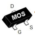
Drain
● ID=-2.8A@VGS=-4.5V
● RDS(on)=69mΩ(Typ.)@VGS=-4.5V
Gate
● RDS(on)=94mΩ(Typ.)@VGS=-2.5V
● RDS(on)=130mΩ(Typ.)@VGS=-1.8V
● Low Gate charge
● Fast switching speed
● Improved dv/dt capability
G. Gate
S. Source
D. Drain
● Suit for -1.8V gate drive applications
JS
● Application:
Source
P-MOS
Note Book
-
Load Switch
-
Hand Held Instruments
-
Switching Appliance
-
Power Management
MI
-
CR
● Lead free and green devices are available
O
● Package: SOT23-3L
Se
Absolute Maximum Ratings (TA=25ºC unless otherwise noted)
mi
Parameter
Drain-Source Voltage
Limit
Unit
VDS
-20
V
±10
V
co
Gate-Source Voltage
VGS
TC=25ºC
TC=25ºC, t ≤ 5s
a
ID
TC=70ºC
IDM
Power Dissipation (TC=25ºC)
Operating Junction Temperature Range
Thermal Resistance, Junction-to-Ambient1
-1.56
A
1.56
W
0.012
W/ºC
TSTG
-55 ~ +150
ºC
TJ
-55 ~ +150
ºC
RθJA
100
ºC/W
r
to
Storage Temperature Range
A
-10.4
PD
Power Dissipation – Derate Above 25ºC
-3.3
uc
Drain Current –Pulsed
a
-2.6
nd
Drain Current
Symbol
eElectrical Characteristics (TJ=25ºC unless otherwise noted)
Parameter
Symbol
Condition
Min
Typ
Max
Unit
Off Characteristics
Drain-Source Breakdown Voltage
Zero Gate Voltage
Drain Current
TJ=25°C
Gate-Body Leakage
On Characteristics
BVDSS
VGS=0V, ID=-250µA
-20
---
---
V
IDSS
VDS=-16V, VGS=0V
---
---
-1
μA
IGSS
VGS=±10V, VDS=0V
---
---
±100
nA
VGS(th)
VDS=VGS, ID=-250µA
-0.3
-0.6
-1.0
V
a
Gate Threshold Voltage
www.jsmsemi.com
第1/4页
�JSM2301SL
-20V P-Channel Enhancement-Mode MOSFET
Drain-Source On-State Resistance
VGS=-4.5V, ID=-3.0A
---
69
85
VGS=-2.5V, ID=-2.0A
---
94
120
VGS=-1.8V, ID=-1.0A
---
130
170
gfs
VDS=-10V, ID=-1A
---
2.2
---
S
IS
VG=VD=0V, Force Current
---
---
-2.6
A
VGS=0V, IS=-1A
---
---
-1.3
V
---
350
510
---
65
95
---
50
75
---
4.8
8
---
0.5
1
RDS(on)
Forward Transconductance
Drain-Source Diode Characteristics
mΩ
a
Continuous Source Current
Diode Forward Voltage
VSD
Dynamic Characteristics b
Input Capacitance
Ciss
Output Capacitance
Coss
Reverse Transfer Capacitance
JS
Switching Characteristics
VDS=-15V, VGS=0V, F=1MHz
Crss
b
Total Gate Charge
Qg
MI
VDS=-10V, VGS=-4.5V,
ID=-2.6A
Qgs
Gate-Drain Charge
Qgd
---
1.9
4
Td(on)
---
3.5
7
---
12.6
24
---
32.5
62
---
8.4
16
Rise Time
Fall Time
Tr
VDD=-10V, VGS=-4.5V,
RG=25Ω, ID=-1A
O
Turn-Off Delay Time
CR
Gate-Source Charge
Turn-On Delay Time
pF
Td(off)
Tf
nC
ns
Se
Notes: a. Repetitive Rating: Pulsed width limited by maximum junction temperature.
b. Pulse test: pulse width ≤ 300us, duty cycle ≤ 2%.
c. Guaranteed by design, not subject to production testing.
mi
Switching Time Test Circuit and Waveforms
r
to
uc
nd
co
www.jsmsemi.com
第2/4页
�JSM2301SL
-20V P-Channel Enhancement-Mode MOSFET
Soldering Methods For Products
1.
2.
Storage environment : Temperature=10ºC~35ºC, Humidity=65%±15%
Reflow soldering of surface mount devices
JS
MI
CR
Figure : Temperature Profile
O
Profile Feature
Average ramp-up rate (TL to TP)
Preheat
- Temperature Min (TSmin)
- Temperature Max (TSmax)
- Time (Min to Max) (ts)
TSmax to TL
- Ramp-up rate
Time maintained above:
- Temperature (TL)
- Time (tL)
Peak Temperature (TP)
Time within 5ºC of actual Peak Temperature (tP)
Ramp-down rate
Time 25ºC to Peak Temperature
Pb-Free Assembly
< 3ºC/sec
100ºC
150ºC
60 ~ 120 sec
100ºC
200ºC
60 ~ 180 sec
Se
Sn-Pb Eutectic Assembly
< 3ºC/sec
mi
< 3ºC/sec
183ºC
60 ~ 150 sec
240ºC +0/-5ºC
10 ~ 30 sec
< 6ºC/sec
< 6 minutes
217ºC
60 ~ 150 sec
260ºC +0/-5ºC
20 ~ 40 sec
< 6ºC/sec
< 8 minutes
3. Flow (wave) soldering (solder dipping)
Product
Peak Temperature
245ºC ±5ºC
260ºC +0/-5ºC
Notices:
Dipping Time
5sec ±1sec
5sec ±1sec
r
to
Pb devices
Pb-Free devices
uc
nd
co
< 3ºC/sec
- All companies, brands, logos, pictures, product names and trademarks are the property of owner respective companies.
- 规格书内容、版本或參数规格如有更改恕不另行通知,如有特定规格的需求请事先告知,如因此而造成任何的问题,供应商不
承担任何赔偿和法律责任。
- MOS 管电路是静电敏感元器件,且对生产环境要求较严,建议在存放、运输及生产操作时一定要避免静电干扰。
- 经锡炉或回焊炉的温度切勿超过 260 ºC。
www.jsmsemi.com
第3/4页
�JSM2301SL
-20V P-Channel Enhancement-Mode MOSFET
PACKAGE OUTLINE
Plastic surface mounted package
SOT-23-3L
SOT-23-3L
O
CR
MI
JS
Dim
Min
Max
A
2.80
3.00
B
1.50
1.70
C
1.00
1.20
D
0.35
0.45
E
0.35
0.55
G
1.80
2.00
H
0.02
0.10
J
0.10
0.20
K
2.60
3.00
All Dimensions in mm
Unit : mm
r
to
uc
nd
co
mi
Se
SOLDERING FOOTPRINT
PACKAGE INFORMATION
Device
Package
Shipping
JSM2301SL
SOT-23-3L
3000/Tape&Reel
www.jsmsemi.com
第4/4页
�
很抱歉,暂时无法提供与“JSM2301SL”相匹配的价格&库存,您可以联系我们找货
免费人工找货