JSM3401L
P-Channel 30-V(D-S) MOSFET
V(BR)DSS
RDS(on)MAX
ID
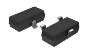
SOT-23-3L
0.053Ω@-10V
-30V
0.065Ω@-4.5V
3
-4.2A
1.GATE
2.SOURCE
0.085Ω@-2.5V
1
3.DRAIN
2
JS
Equivalent Circuit
MI
General FEATURE
●TrenchFET Power MOSFET
●Lead free product is acquired
●Surface mount package
CR
O
APPLICATION
●Load Switch for Portable Devices
●DC/DC Converter
mi
Se
Maximum ratings (Ta=25℃ unless otherwise noted)
co
Parameter
Value
Symbol
Gate-Source Voltage
VGS
Continuous Drain Current
ID
Pulsed Drain Current
IDM
Maximum Power Dissipation
PD
Thermal Resistance from Junction to Ambient(t ≤5s)
R θJA
-30
-4.2
-30
A
1.25
W
95
℃/W
Junction Temperature
TJ
150
Storage Temperature
Tstg
-55 ~+150
www.jsmsemi.com
V
±12
r
to
uc
VDS
nd
Drain-Source Voltage
Unit
℃
第1/6页
�JSM3401L
P-Channel 30-V(D-S) MOSFET
MOSFET ELECTRICAL CHARACTERISTICS
Ta =25 ℃ unless otherwise specified
Parameter
Symbol
Test Condition
Min
Typ
Max
Units
Static characteristics
BVDSS
VGS = 0V, ID =-250µA
Zero gate voltage drain current
IDSS
VDS =-24V,VGS = 0V
-1
µA
Gate-source leakage current
IGSS
VGS =±12V, VDS = 0V
±100
nA
Drain-source breakdown voltage
RDS(on)
JS
Drain-source on-resistance (note a)
MI
Forward tranconductance (note a)
gFS
VGS(th)
Gate threshold voltage
CR
Diode forward voltage (note a)
VSD
V
-30
VGS =-10V, ID =-4.0A
50
53
mΩ
VGS =-4.5V, ID =-3.5A
60
65
mΩ
VGS =-2.5V, ID =-2.5A
80
85
mΩ
VDS =-5V, ID =-4.2A
7
10
VDS =VGS, ID =-250µA
-0.6
-1
IS=-1A,VGS=0V
S
-1.2
V
-1.2
V
Dynamic characteristics (note b)
O
Input capacitance
Ciss
Coss
Reverse transfer capacitance
Crss
Switching Characteristics (note b)
Turn-on rise time
Turn-off fall time
pF
115
pF
75
pF
7.0
ns
tr
VGS=-10V,VDS=-15V,
3.0
ns
td(off)
ID =-4.2A ,RGEN=6Ω
30
ns
12
ns
tf
b.These parameters have no way to verify.
www.jsmsemi.com
r
to
uc
a.Pulse Test : Pulse Width < 300µs, Duty Cycle ≤2%.
nd
Notes:
co
Turn-off delay time
td(on)
mi
Turn-on delay time
VDS =-15V, VGS = 0 V, f =1MHz
Se
Output capacitance
950
第2/6页
�JSM3401L
P-Channel 30-V(D-S) MOSFET
Typical Electrical and Thermal Characteristics
ton
tr
td(on)
toff
tf
td(off)
90%
VOUT
90%
INVERTED
10%
10%
90%
VIN
50%
JS
10%
PULSE WIDTH
MI
Figure 1:Switching Test Circuit
O
co
mi
Se
ID- Drain Current (A)
Figure 2:Switching Waveforms
CR
PD Power(W)
50%
TJ-Junction Temperature(℃)
nd
TJ-Junction Temperature(℃)
Figure 3 Power Dissipation
Figure 4 Drain Current
ID- Drain Current (A)
Rdson On-Resistance(mΩ)
r
to
uc
Vds Drain-Source Voltage (V)
Figure 5 Output Characteristics
ID- Drain Current (A)
Figure 6 Drain-Source On-Resistance
www.jsmsemi.com
第3/6页
�JSM3401L
Normalized On-Resistance
JS
ID- Drain Current (A)
P-Channel 30-V(D-S) MOSFET
TJ-Junction Temperature(℃)
Figure 7 Transfer Characteristics
Figure 8 Drain-Source On-Resistance
co
mi
Se
C Capacitance (pF)
O
CR
Rdson On-Resistance(mΩ)
MI
Vgs Gate-Source Voltage (V)
nd
Vds Drain-Source Voltage (V)
r
to
uc
Vgs Gate-Source Voltage (V)
Figure 10 Capacitance vs Vds
Vgs Gate-Source Voltage (V)
Is- Reverse Drain Current (A)
Figure 9 Rdson vs Vgs
Qg Gate Charge (nC)
Figure 11 Gate Charge
Vsd Source-Drain Voltage (V)
Figure 12 Source- Drain Diode Forward
www.jsmsemi.com
第4/6页
�JSM3401L
JS
ID- Drain Current (A)
P-Channel 30-V(D-S) MOSFET
MI
CR
Vds Drain-Source Voltage (V)
O
co
mi
Se
r
to
uc
nd
r(t),Normalized Effective
Transient Thermal Impedance
Figure 13 Safe Operation Area
Square Wave Pluse Duration(sec)
Figure 14 Normalized Maximum Transient Thermal Impedance
www.jsmsemi.com
第5/6页
�JSM3401L
P-Channel 30-V(D-S) MOSFET
SOT-23 -3L Package Outline Dimensions
JS
MI
Dimensions In Millimeters
Min.
Max.
1.050
1.250
0.000
0.100
1.050
1.150
0.300
0.500
0.100
0.200
2.820
3.020
1.500
1.700
2.650
2.950
0.950(BSC)
1.800
2.000
0.300
0.600
0°
8°
Dimensions In Inches
Min.
Max.
0.041
0.049
0.000
0.004
0.041
0.045
0.012
0.020
0.004
0.008
0.111
0.119
0.059
0.067
0.104
0.116
0.037(BSC)
0.071
0.079
0.012
0.024
0°
8°
O
r
to
uc
nd
SOT-23-3L Suggested Pad Layout
co
mi
Se
A
A1
A2
b
c
D
E1
E
e
e1
L
�
CR
Symbol
www.jsmsemi.com
第6/6页
�
很抱歉,暂时无法提供与“JSM3401L”相匹配的价格&库存,您可以联系我们找货
免费人工找货