JSM4407
P-Channel Enhancement Mode Power MOSFET
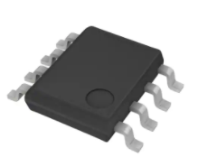
SOP-8
Description
S
1
8
D
S
7
D
excellent RDS(ON), low gate charge and operation with gate
2
S
3
6
D
voltages as low as 4.5V.
G
4
5
D
The JSM4407 uses advanced trench technology to provide
Top View
General Features
or
Equiva len t Cir cu it
● VDS = -30V
RDS(ON) < 20mΩ @ VGS=-4.5V I D = -6.0A
G
ct
RDS(ON) < 14mΩ @ VGS=-10V
S
I D = -10.0A
du
● High power and current handing capability
● Lead free product is acquired
D
MARKING
on
● Surface mount package
Application
ic
● Battery Switch
● Load switch
YW
o
em
● Power management
4407
S
Y :year code W :week code
Absolute Maximum Ratings (TA=25℃unless otherwise noted)
Parameter
Symbol
Drain-Source Voltage
VDS
Gate-Source Voltage
VGS
Unit
-30
V
±20
V
ID
-10
A
(Note 1)
IDM
-60
A
Maximum Power Dissipation
PD
2.1
W
TJ,TSTG
-55 To 150
℃
RθJA
50
℃/W
MI
CR
O
Limit
JS
Continuous Drain Current (TJ =150℃)
Drain Current-Pulsed
TA =25℃
Operating Junction and Storage Temperature Range
Thermal Characteristic
Thermal Resistance,Junction-to-Ambient
(Note 2)
www.jsmsemi.com
第1/6页
�JSM4407
P-Channel Enhancement Mode Power MOSFET
Electrical Characteristics (TA=25℃unless otherwise noted)
Parameter
Symbol
Condition
Min Typ
Max
Unit
Drain-Source Breakdown Voltage
BVDSS
VGS=0V ID=-250μA
-30
-
-
V
Zero Gate Voltage Drain Current
IDSS
VDS=-30V,VGS=0V
-
-
-1
μA
Gate-Body Leakage Current
IGSS
VGS=±20V,VDS=0V
-
-
±100
nA
Gate Threshold Voltage
VGS(th)
VDS=VGS,ID=-250μA
-1
-
-3.0
V
Drain-Source On-State Resistance
RDS(ON)
VGS=-10V, ID=-10.0A
-
9
14
mΩ
Off Characteristics
14
20
mΩ
20
-
-
S
-
1750
-
PF
-
215
-
PF
-
180
-
PF
-
9
-
nS
VDD=-15V, ID=-10A,
-
8
-
nS
VGS=-10V,RGEN=1Ω
-
28
-
nS
10
-
nS
-
24
-
nC
-
3.5
-
nC
-
6
-
nC
-
-
-1.2
V
VDS=-15V,ID=-5.0A
Clss
Output Capacitance
Coss
Reverse Transfer Capacitance
Switching Characteristics
uc
(Note4)
Input Capacitance
VDS=-15V,VGS=0V,
F=1.0MHz
Crss
(Note 4)
Turn-on Delay Time
td(on)
Turn-on Rise Time
tr
td(off)
mi
Turn-Off Delay Time
Turn-Off Fall Time
tf
Qg
Se
Total Gate Charge
Gate-Source Charge
Qgs
Qgd
RO
Gate-Drain Charge
r
-
nd
Dynamic Characteristics
gFS
to
Forward Transconductance
VGS=-4.5V, ID=-6.0A
co
On Characteristics
(Note 3)
VDS=-15V,ID=-10.0A
VGS=-10V
Drain-Source Diode Characteristics
Notes:
(Note 3)
VSD
VGS=0V,IS=-10A
MI
C
Diode Forward Voltage
JS
1. Repetitive Rating: Pulse width limited by maximum junction temperature.
2. Surface Mounted on FR4 Board, t ≤ 10 sec.
3. Pulse Test: Pulse Width ≤ 300μs, Duty Cycle ≤ 2%.
4. Guaranteed by design, not subject to production
www.jsmsemi.com
第2/6页
�JSM4407
P-Channel Enhancement Mode Power MOSFET
Typical Electrical and Thermal Characteristics
ton
tr
td(on)
toff
tf
td(off)
90%
VOUT
90%
INVERTED
10%
10%
50%
or
90%
VIN
50%
10%
ct
PULSE WIDTH
Figure 2:Switching Waveforms
MI
CR
O
S
em
ic
PD Power(W)
ID- Drain Current (A)
on
du
Figure 1:Switching Test Circuit
TJ-Junction Temperature(℃)
TJ-Junction Temperature(℃)
Figure 4 Drain Current
Rdson On-Resistance(Ω)
JS
ID- Drain Current (A)
Figure 3 Power Dissipation
ID- Drain Current (A)
Vds Drain-Source Voltage (V)
Figure 5 Output Characteristics
Figure 6 Drain-Source On-Resistance
www.jsmsemi.com
第3/6页
�or
ct
ID- Drain Current (A)
Normalized On-Resistance
JSM4407
P-Channel Enhancement Mode Power MOSFET
TJ-Junction Temperature(℃)
du
Vgs Gate-Source Voltage (V)
Figure 8 Drain-Source On-Resistance
MI
CR
O
S
em
ic
C Capacitance (pF)
on
Rdson On-Resistance(Ω)
Figure 7 Transfer Characteristics
Vgs Gate-Source Voltage (V)
Vds Drain-Source Voltage (V)
Figure 10 Capacitance vs Vds
Is- Reverse Drain Current (A)
JS
Vgs Gate-Source Voltage (V)
Figure 9 Rdson vs Vgs
Qg Gate Charge (nC)
Figure 11 Gate Charge
Vsd Source-Drain Voltage (V)
Figure 12 Source- Drain Diode Forward
www.jsmsemi.com
第4/6页
�du
Vds Drain-Source Voltage (V)
ct
or
ID- Drain Current (A)
JSM4407
P-Channel Enhancement Mode Power MOSFET
ic
em
S
MI
CR
O
r(t),Normalized Effective
Transient Thermal Impedance
on
Figure 13 Safe Operation Area
JS
Square Wave Pluse Duration(sec)
Figure 14 Normalized Maximum Transient Thermal Impedance
www.jsmsemi.com
第5/6页
�JSM4407
P-Channel Enhancement Mode Power MOSFET
MI
CR
O
S
em
ic
on
du
ct
or
SOP-8 Package Information
Dimensions In Millimeters
Dimensions In Inches
Min.
Max.
Min.
Max.
1.350
1.750
0.053
0.069
A1
0.100
0.250
0.004
0.010
A2
1.350
1.550
0.053
0.061
b
0.330
0.510
0.013
0.020
JS
Symbol
0.170
0.250
0.006
0.010
D
4.700
5.100
0.185
0.200
E
3.800
4.000
0.150
0.157
E1
5.800
6.200
0.228
0.244
A
c
e
1.270(BSC)
0.050(BSC)
L
0.400
1.270
0.016
0.050
θ
0°
8°
0°
8°
www.jsmsemi.com
第6/6页
�
很抱歉,暂时无法提供与“JSM4407”相匹配的价格&库存,您可以联系我们找货
免费人工找货