DPC-817
4 PIN DIP PHOTOTRANSISTOR PHOTOCOUPLER
General Description
Features
●The DPC-817 series are optically coupled isolators
●Current transfer ratio (CTR: 50~600% at IF =5mA,
containing a GaAs light emitting diode and an NPN
VCE =5V)
●High isolation voltage between input and output
silicon phototransistor
(Viso=5000 Vrms )
●The lead pitch is 2.54mm
●Creepage distance >7.62 mm
●Operating temperature up to +110°C
● Compact small outline package
Rank Table Of Current Transfer Ratio (CTR)
●UL approved (No.E343249)
RANK MARK.
Min. ( %)
Max. ( %)
L
50
100
A
80
160
Applications
B
130
260
● Computer terminals.
C
200
400
D
300
600
50
600
L or A or B or C or D
Notes:
●Pb free and RoHS compliant.
● System appliances, measuring instruments.
● Registers, copiers, automatic vending
machines.
● Electric home appliances, such as fan
heaters, etc, of different potentials and
Conditions: IF=5mA, VCE=5V, Ta=25℃.
impedances.
● Signal transmission between circuits
Pin Configuration
Pin Assignment
Pin num.
Symbol
1
Anode
2
Cathode
3
Emitter
4
Collector
Functions
Input
Output
V01
www.microne.com.cn
Page 1 of 8
�DPC-817
Absolute Maximum Ratings (Ta=25℃)
Symbol
Rating
Unit
Forward Current
IF
50
mA
Reverse Voltage
VR
6
V
Power Dissipation
P
70
mW
Collector-Emitter Voltage
VCEO
35
Emitter- Collector Voltage
VECO
6
Collector Current
IC
50
mA
Collector Power Dissipation
PC
150
mW
Total Power Dissipation
Ptot
200
mW
Isolation Voltage(NOTE)
VISO
5000
Vrms
Rated impulse isolation voltage
VIOTM
6000
V
Rated repetitive peak isolation voltage
VIORM
630
V
operating Junction Temperature TJ
TOPR
-40 to 85
Storage Temperature
TSTQ
-55 to 125
Lead Temperature (Soldering, 10secs)
TSOL
260
Parameter
INPUT
OUTPUT
V
℃
Notes: AC For minute, R.H. =40~60%
Isolation voltage shall be measured using the following method.
(1) Short between anode and cathode on the primary side and between collector and emitter on the secondary side.
(2) The isolation voltage tester with zero-cross circuit shall be used.
(3) The waveform of applied voltage shall be a sine wave.
Caution: The absolute maximum ratings are rated values exceeding which the product could suffer physical damage. These values must
therefore not be exceeded under any conditions.
Block Diagram
V01
www.microne.com.cn
Page 2 of 8
�DPC-817
Electrical Characteristics
(TA =25 °C, unless otherwise noted.)
Item
Symbol
Test condition
Min
Typ
Max
Unit
1.2
1.4
V
10
uA
250
PF
100
nA
Input Section
Forward Voltage
VF
IF=20mA
Reverse Current
IR
VR=4V
Terminal Capacitance
Ct
V=0, f=1KHz
30
Output Section
Collector Dark Current
ICEO
Collector-Emitter
Breakdown Voltage
BVCEO
Emitter-Collector
Breakdown Voltage
BVECO
Transfer
VCE=20V, IF=0
IC=0.1mA
IF=0
IE=10µA
IF=0
35
V
6
V
Characteristic Section
Collector Current
Ic
Current Transfer Ratio(note)
CTR
Collector-Emitter
Saturation Voltage
VCE(sat)
Isolation Resistance
Riso
DC500V
40~60%R.H.
Floating Capacitance
Cf
V=0, f=1MHz
0.6
Cut-Off Frequency
fc
VCE=5V,IC=2mA
RL=100Ω,-3dB
80
Response Time(Rise)
tr
VCE=2V,IC=2mA
Response Time(Fall)
tf
Note:
IF=5mA
VCE=5V
2.5
30
mA
50
600
%
0.2
V
1
pF
IF=20mA
0.1
IC= 1mA
RL=100Ω
5×10¹⁰
1×10¹¹
kHz
4
18
uS
3
18
uS
CTR= IC / IF × 100%
V01
www.microne.com.cn
Page 3 of 8
�DPC-817
Typical performance characteristics
(1) Forward Current vs. Ambient Temperature
(2) Collector Power Dissipation vs. Ambient
Temperature
(3) Collector-emitter Saturation Voltage vs.
Forward Current
(4) Forward Current vs. Forward Voltage
(5) Current Transfer Ratio vs. Forward Current
(6) Collector Current vs. Collector-emitter Voltage
V01
www.microne.com.cn
Page 4 of 8
�DPC-817
(7) Relative Current Transfer Ratio vs.
Ambient Temperature
(9) Collector Dark Current vs.
Ambient Temperature
(11) Frequency Response
V01
(8)Collector-emitter Saturation Voltage vs.
Ambient Temperature
(10) Response Time vs. Load Resistance
Test Circuit for Response Time
www.microne.com.cn
Page 5 of 8
�DPC-817
Reliability Test
Classification
Test Item
Operation Life
High
Temperature
High Humidity
Reverse Bias
(H3TRB)
Endurance
Test
Test Conditions
MIL-STD-750:1026
MIL-STD-883:1005
JIS C 7021 : B-1
JIS C 7021
:B-11
Result
Connect with a power If=50mA
Ta=Under room temperature
Test time=1,000hrs
0/20
Ta=+85℃±5℃, RH=85%
PTR=VCE Absolute max rating*80%
Test time=1000hrs
0/20
0/20
High
Temperature
Reverse Bias
(HTRB)
JIS C 7021 : B- 8
Ta=+105℃±5℃
PTR=VCE absolute max rating
Test time=1000hrs
High
Temperature
Storage
MIL-STD-883:1008
JIS C 7021 :B-10
High Ta=+125℃±5℃
Test time=1,000hrs
0/20
Low Ta=-55℃±5℃
Test time=1,000hrs
0/20
P=15PSIG, Ta=121℃
Humi. =100%RH, 48hrs
0/20
Low Temperature
Storage
Environmental
Test
Reference Standard
JIS-C-7021
:B-12
Autoclave
JESD 22-A102-B
Temperature
Cycling
MIL-STD-202:107D
MIL-STD-750:1051
MIL-STD-883:1010
JIS C 7021 :A-4
125℃ ~ 25℃ ~ -55℃ ~ 25℃
30min 5min
30min 5min
Test Time=20cycle
Thermal Shock
MIL-STD-202:107D
MIL-STD-750:1051
MIL-STD-883:1011
125℃ ~-55℃
20min 20min
Test Time=20cycle
Solder
Resistance
MIL-STD-202:201A
MIL-STD-750:2031
JIS C 7021 :A-1
Solder Ability
MIL-S-883:2003
JIS C 7021
:A-2
0/20
Operation heating:300℃,
0/20
within 10±1seconds.
Operation heating:260℃,
Judgment Criteria Of Failure For The Reliability
Symbol
Measuring conditions
0/20
within 5±1seconds.
Judgment criteria for failure
VF (V)
If=20mA
Over Ux1.0
Ir(uA)
Vr=4V
Over Ux1.0
CTR(%)
If=5mA, VCE=5V
Shift>1.2
VCE(sat)
IF=20mA, IC= 1mA
Over Ux1.0
BVCEO
IC=0.1mA, IF=0
Over Ux1.0
BVECO
IE=10µA, IF=0
Over Ux1.0
V01
www.microne.com.cn
0/20
Page 6 of 8
�DPC-817
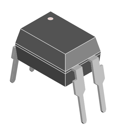
Package Information
Package type:DIP4
Unit:mm(inch)
Dimension (mm)
Dimension (Inches)
Character
Min
Max
Min
Max
A
6.200
6.600
0.244
0.260
B
4.280
4.880
0.169
0.192
C
0.300(Typ.)
D
7.620
9.500
0.300
0.374
E
4.200
4.800
0.165
0.189
F
2.300
3.300
0.090
0.130
a
1.2
1.4
0.047
0.055
b
0.3
0.5
0.012
0.020
c
0.4
0.6
0.016
0.024
d
2.54Typ.)
0.060(Typ.)
e
0.25(Typ.)
(Typ.)
θ
V01
7.620(Typ.)
00
150
www.microne.com.cn
00
150
Page 7 of 8
�DPC-817
z
z
z
z
z
The information described herein is subject to change without notice.
Nanjing Micro One Electronics Inc is not responsible for any problems caused by circuits or
diagrams described herein whose related industrial properties, patents, or other rights
belong to third parties. The application circuit examples explain typical applications of the
products, and do not guarantee the success of any specific mass-production design.
Use of the information described herein for other purposes and/or reproduction or copying
without the express permission of Nanjing Micro One Electronics Inc is strictly prohibited.
The products described herein cannot be used as part of any device or equipment affecting
the human body, such as exercise equipment, medical equipment, security systems, gas
equipment, or any apparatus installed in airplanes and other vehicles, without prior written
permission of Nanjing Micro One Electronics Inc.
Although Nanjing Micro One Electronics Inc exerts the greatest possible effort to ensure
high quality and reliability, the failure or malfunction of semiconductor products may occur.
The user of these products should therefore give thorough consideration to safety design,
including redundancy, fire-prevention measures, and malfunction prevention, to prevent any
accidents, fires, or community damage that may ensue.
V01
www.microne.com.cn
Page 8 of 8
�