JSM501-JSM511
High Voltage Hall Effect Switch Family
Vinbelltech
Co. Ltd
Introduction
to
r
JSM50X family consists of different Hall switches produced in BCDMOS technology. All
Hall sensors include a temperature-compensated Hall plate with active offset compensation, a comparator,
and an output driver. The family consists of 3-wire devices, the corresponding output driver being an opendrain output transistor and a current source respectively. The comparator compares the actual magnetic flux
with the fixed reference values (switching points). Accordingly the output transistor is switched on or off in
3-wire version. The active offset compensation leads to constant magnetic characteristics over supply
voltage and temperature range. In addition, the magnetic parameters are robust against mechanical stress
effects.
The sensors are designed for industrial and automotive applications and operate with supply voltages from 2.7
V to 30V in ambient temperature range from -40 °C up to 150 °C.
uc
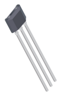
The family JSM50X is available in SOT-23 and the leaded version TO92S packages.
Features
Applications
nd
Speed and RPM sensing
Tachometer, counter pickup
Flow-rate sensing
Brushless dc motor commutation
Motor and fan control
Robotics control
Proximity sensor
Position sensor
Seat position detection
Seat belt buckles
Hood/trunk/door latches
Sun
roof/convertible
top/tailgate/liftgate
actuation
Brake/clutch pedals
Electric power steering (EPS)
Transmissions and shift selectors
Wiper motor
co
mi
Se
CR
O
JS
MI
SOT-23 and TO92S packages
Low current consumptions of typ. 2.5 mA
Operates from 2.7 V to 30 V supply voltage
Overvoltage protection capability up to 40 V
Highest ESD performance up to ±12 kV
Short-circuit protected open-drain output and
thermal shut down for 3-wire applications
Magnetic characteristics are robust regarding
mechanical stress effects
Constant switching points over a wide supply
voltage and temperature range
Wide operating temperature range from -40 °C
to 150 °C
The decrease of magnetic flux density caused by
rising temperature in the sensor system is
compensated by a built-in negative temperature
coefficient of the magnetic characteristics
Reverse-voltage protection at Vcc pin
Ideal sensor for applications in extreme
automotive and industrial environments
Qualified according to AEC-Q100 test standard for
automotive electronics industry to provide the
highest quality expectation
Package
SOT23
www.jsmsemi.com
TO92
第1页,共15页
�JSM501-JSM511
High Voltage Hall Effect Switch Family
Contents
Title
Page
JSM50X Family Overview
3
2.
Ordering Information
5
2.1
Marking Code
2.2
Operating Ambient Temperature Range
2.3
Hall Sensor Package Codes
3.
Functional Description
4.
Diagnostic Features
5.
Specifications
5.1
Outline Dimensions
5.2
Pin assignment
5.3
Absolute Maximum Ratings
5.4
ESD and Latch-up
11
5.5
Recommended Operating Conditions
11
5.6
Characteristics
12
5.7
Magnetic Characteristics Overview
13
6.
Magnetoelecric conversion characteristics
13
7.
Application circui
14
to
r
1.
CR
O
Section
6
JS
MI
Se
mi
co
nd
uc
6
www.jsmsemi.com
6
6
7
8
8
10
10
第2页,共15页
�JSM501-JSM511
High Voltage Hall Effect Switch Family
1. JSM50X Family Overview
The types within each family differ according to the magnetic flux density values for the magnetic switching points, the
temperature behavior of the magnetic switching points, the mode of switching, the number of pins and the average
current consumption. Table 1 to Table 4 list some devices classified in terms of switching behavior and sensitivity: higher
Table 1: JSM50X 3-wire devices
co
nd
Sensitivity
Very high
Very high
Very high
High
Medium
Medium
Low
High
High
Medium
Medium
Se
mi
Switching Behavior
Bipolar
Latching
Unipolar
Latching
Latching
Unipolar
Uipolar
Unipolar
Unipolar inverted
Unipolar
Unipolar
JS
MI
CR
O
Type Sensitivity
JSM501
JSM502
JSM503
JSM504
JSM505
JSM506
JSM507
JSM508
JSM509
JSM510
JSM511
uc
to
r
sensitivity correlates to lower switching points.
The following definitions outline the device behavior for different switching points:
Latching Sensors:
3-wire: The output turns low with the magnetic south pole on the branded side of the package and turns high with the
magnetic north pole on the branded side.
The output does not change if the magnetic field is removed. For changing the output state, the opposite magnetic
field polarity must be applied.
www.jsmsemi.com
第3页,共15页
�JSM501-JSM511
High Voltage Hall Effect Switch Family
Output Voltage
VOH
BHYS
VOL
Bop
0
B
to
r
Brp
Fig. 1: Definition of magnetic switching points for 3- wire latching sensor.
uc
Bipolar Switching Sensors (3-wire only):
The output turns low with the magnetic south pole on the branded side of the package and turns high with the magnetic
nd
north pole on the branded side. The output state is not defined if the magnetic field is removed again. Some sensors will
change the output state and some sensors will not.
mi
co
Output Voltage
VOH
Se
BHYS
VOL
0
Bop
B
JS
MI
CR
O
Brp
www.jsmsemi.com
第4页,共15页
�JSM501-JSM511
High Voltage Hall Effect Switch Family
Vinbelltech
Co.ofLtd
Fig. 2: Definition
magnetic switching points for 3- wire bipolar sensor.
Unipolar Switching Sensors:
3-wire: The output turns low with the magnetic south pole on the branded side of the package and turns high if the
mi
co
nd
uc
to
r
magnetic field is removed. The sensor does not respond to the magnetic north pole on the branded side.
Se
Fig. 3: Definition of magnetic switching points for 3-wire unipolar sensor.
Unipolar Switching Sensors with Inverted Output:
CR
O
3-wire: The output turns high with the magnetic south pole on the branded side of the package and turns low if the
JS
MI
magnetic field is removed. The sensor does not respond to the magnetic north pole on the branded side.
Fig. 4: Definition of magnetic switching points for 3- wire unipolar sensor with inverted output.
2. Ordering Information
www.jsmsemi.com
第5页,共15页
�JSM501-JSM511
High Voltage Hall Effect Switch Family
Vinbelltech
2.1. MarkingCo.
Code Ltd
All Hall sensors have a marking on the package surface (branded side). This marking includes the name of the sensor and
date code.
2.2. Operating Ambient Temperature Range
The Hall sensors from Vinbelltech are specified to the ambient temperature.
to
r
TA = -40 °C up to 150 °C
2.3. Hall Sensor Package Codes
uc
Hall sensors are available in a wide variety of packaging versions and quantities.
nd
Ordering information
Package
Packing
JSM50X
TO92S
Bulk, 1000 pieces/bag
JSM50X
SOT23
Tape&Reel, 3000 pieces/reel
Ambient, TA
-40℃ to 150℃
-40℃ to 150℃
CR
O
Se
mi
co
Part number
3. Functional Description
JS
MI
JSM50X Hall effect sensor switches are available with different magnetic switching levels and output polarity.
JSM50X sensors are monolithic integrated circuits which switch in response to magnetic fields. If a magnetic field with
flux lines perpendicular to the sensitive area is applied to the sensor, the biased Hall plate forces a Hall voltage
proportional to this field.
The Hall voltage is compared with the actual threshold level in the comparator. If the magnetic field exceeds the
threshold levels, the output stage (open drain output for 3-wire devices or current source for 2-wire devices) is switched
to the appropriate state. The built-in hysteresis eliminates oscillation and provides switching behavior of output without
bouncing.
Magnetic offset caused by mechanical stress is compensated by using the chopping offset compensation technique. A
serial resistor or diode on the supply line is not required thanks to the built-in reverse voltage protection.
www.jsmsemi.com
第6页,共15页
�JSM501-JSM511
High Voltage Hall Effect Switch Family
Vinbelltech
Co.output
Ltd is forced to a safe, high-impedance state (tri-state), in any of the following fault conditions:
The open drain
overtemperature, and undervoltage. In addition, the output current is limited (short-circuit protection).
The device is able to withstand a maximum supply voltage of 28 V for unlimited time and features overvoltage capability
Se
CR
O
Fig. 5: JSM50x- 3-wire - Block diagram
mi
co
nd
uc
to
r
(40V load dump).
4. Diagnostic Features
JS
MI
Internal states are monitored and in an error condition flagged with a tri-state at the output (3-wire devices):
– Internal voltage regulator: under and over voltage detection
– Monitoring of internal bias and current levels
– Monitoring of the internal reference voltage
– Monitoring of the Hall plate voltage
www.jsmsemi.com
第7页,共15页
�Vinbelltech
Co. Ltd
5. Specifications
5.1. Outline Dimensions
Symbol
Size (mm)
minimum
maximum
1.42
1.67
0.66
0.86
0.35
0.56
0.4
0.55
0.36
0.51
3.9
4.2
2.97
3.27
2.9
3.28
1.270 TYP
2.44
2.64
13.5
15.5
2.025TYP
1.545TYP
0.500TYP
45˚TYP
JS
MI
A
A1
b
b1
C
D
D1
E
e
e1
L
x
y
z
θ
CR
O
TO92S dimensions
Se
mi
co
nd
uc
to
r
TO92S
Size (in inches)
minimum
maximum
0.056
0.066
0.026
0.034
0.014
0.022
0.016
0.022
0.014
0.02
0.154
0.165
0.117
0.129
0.114
0.129
0.050 TYP
0.096
0.104
0.531
0.61
0.080TYP
0.061TYP
0.020TYP
45˚TYP
www.jsmsemi.com
第8页,共15页
�JSM501-JSM511
High Voltage Hall Effect Switch Family
nd
(0~9) (1~52)
1.05
1.25
A1
0
0.1
A2
1.05
1.15
b
0.3
c
D
mi
A
Size (in inches)
minimum
minimum
0.041
0.049
Se
Size (mm)
maximu
minimum
m
co
SOT23 dimensions
Symbol
0.004
0.041
0.045
0.5
0.012
0.02
0. 100
0.2
0.004
2.82
3.02
0.111
0.119
0.008
E
1.5
1.7
0.059
0.067
E1
2.65
2.95
0.104
0.116
JS
MI
CR
O
0
e
0.950 TYP
0.037 TYP
e1
1.8
2
0.071
0.079
L
0.3
0.6
0.012
0.024
x
1.460TYP
0.057TYP
y
0.800TYP
0.032TYP
z
0.600TYP
0.024TYP
θ
0˚
uc
to
r
Vinbelltech Co. Ltd
8˚
0˚
8˚
www.jsmsemi.com
第9页,共15页
�JSM501-JSM511
High Voltage Hall Effect Switch Family
TO92S
SOT23
mi
Fig.6: Pin assignment of TO92S and SOT23
co
nd
uc
to
r
Vinbelltech
Co. Ltd
5.2. Pin assignment
Name
1
2
3
VCC
GND
Vout
Function
Power supply
Ground
Output
JS
MI
CR
O
Pin number
Se
Pin assignment
5.3. Absolute Maximum Ratings
Stresses beyond those listed in the “Absolute Maximum Ratings” may cause permanent damage to the device. This is a
stress rating only. Functional operation of the device at these conditions is not implied. Exposure to absolute maximum
rating conditions for extended periods will affect device reliability.
This device contains circuitry to protect the inputs and outputs against damage due to high static voltages or electric
fields; however, it is advised that normal precautions be taken to avoid application of any voltage higher than absolute
maximum-rated voltages to this circuit.
All voltages listed are referenced to ground (GND).
www.jsmsemi.com
第10页,共15页
�JSM501-JSM511
High Voltage Hall Effect Switch Family
Vinbelltech
Ltd
Symbol Co. Parameter
VCC
Supply voltage
Pin No
Min.
20
1
Max.
Unit
Conditions
V
t < 1000 h 1)
34
V
t < 96 h1)
36
V
t < 5 min1)
40
V
t < 5 x 400 ms1)
Output voltage
0.5
3
V
34
V
36
V
3
IOR
Reverse output
current
3
TA
Ambient temperature
range
5.4. ESD and Latch-up
t < 5 min1)
mA
mA
170
°C
t < 5 x 400 ms1)
with series resistor RL > 100
t < 96 h1)
Se
No cumulative stress
40
t < 96 h1)
CR
O
1)
50
65
co
Output current
mi
IO
V
nd
40
t < 1000 h1)
uc
VOUT
to
r
with series resistor RV > 100
The output pin has to be in tri-state (high impedance) for ESD measurements.
JS
MI
ESD and latch-up
Symbol
Parameter
Min
Max
Unit
Ilatch
Maximum latch-up free current at any pin (measurement
according to AEC Q100-004), class 1
100
100
mA
VHBM
Human body model (according to AEC Q100-002)
12
kV
5.5. Recommended Operating Conditions
Functional operation of the device beyond those indicated in the “Recommended Operating Conditions” of this
specification is not implied, may result in unpredictable behavior of the device and may reduce reliability and
lifetime.
All voltages listed are referenced to ground (GND).
www.jsmsemi.com
第11页,共15页
�JSM501-JSM511
High Voltage Hall Effect Switch Family
Parameter
VCC
Supply voltage
TA
Ambient temperature
range
VOUT
Output voltage
IOUT
Output current
Pin No
1
Min
Typ
Max
Unit
2.7
30
V
40
150
°C
3
30
V
3
25
mA
3-wire
uc
5.6. Characteristics
Conditions
to
r
Symbol
at TA = -40 °C to 150 °C, VCC = 3.0 V to 24 V, at Recommended Operation Conditions if not otherwise
Symbol
Parameter
Pin No
Supply current
IccR
Reverse current
Port Output
3
Max
Unit
2.5
3.2
mA
3-wire
1
mA
for Vcc = -18 V
0.4
V
IO = 20 mA
0.5
V
IO = 25 mA
1
µs
0.13
Output fall time
JS
MI
tf
Port low output voltage
CR
O
Vol
1
Typ
Se
Icc
Min
mi
Supply
co
nd
specified in the column “Conditions”. Typical Characteristics for TA= 25 °C and VCC = 12 V
tr
Output rise time
Bnoise
Effective noise of
magnetic switching
points
tj
Output jitter
td
Delay time
tsamp
Output refresh period
ten
Enable time of output after
settling of Vcc
Conditions
Vcc = 12V; RL =
820 ; CL = 20 pF
1
0.1
0.5
16
1.6
2
50
µs
mT
For square wave signal
with 1 kHz
µs
For square wave signal
with 1 kHz
µs
2.66
µs
µs
VCC = 12V
B > Bon + 2 mT or
B < Boff - 2 mT
www.jsmsemi.com
第12页,共15页
�JSM501-JSM511
High Voltage Hall Effect Switch Family
5.7. Magnetic Characteristics Overview
TA = -40 °C to 150 °C, Vcc = 3.0 V to 30 V, GND = 0 V, recommended operation conditions if not otherwise specified in the
column “Conditions”. Typical characteristics for TA= 25 °C.
On point BON
[mT]
TC
Min
[ppm/K]
Typ
Off point BOFF
[mT]
Max
Min
3-wire
JSM501
bipolar
0
JSM502
latching
1000
2.5
JSM503
unipolar
1000
5.5
JSM504
latching
JSM505
latching
JSM506
unipolar
-1000
JSM507
unipolar
300
JSM508
unipolar
JSM509
unipolar
JSM510
unipolar
JSM511
unipolar
1) [mT]
Max
Min
0.9
nd
uc
0.9
co
Typ
Hysteresis BHYS
to
r
Sensor
Switching
Type
Temp. coeff. of
magnetic thresh.
Typ
1.8
2.5
5.0
3.5
2.0
16.0
2.0
27.0
23.0
4.0
1000
5.5
3.5
2.0
1000
3.5
5.5
2.0
1000
10
8
2.0
1000
8
10
2.0
JS
MI
CR
O
Se
mi
18.0
Max
6. Magnetoelectric conversion characteristics
Apply a magnetic field greater than Bop on the seal side of TO92S package (near the South Pole),
and the output becomes low;Apply a magnetic field less than Brp (near the North Pole) and the
output becomes high.When the chip is first powered on, if the magnetic field is between the Bop
and the Brp, the output state is in an undefined state (high or low).The magnetic field polarity of
the operating and releasing points of SOT23 package is opposite to that of TO92S.See below.
www.jsmsemi.com
第13页,共15页
�JSM501-JSM511
High Voltage Hall Effect Switch Family
Vinbelltech Co. Ltd
Output Voltage
VOH
BHYS
VOL
VOUT=high
B
TO92S output state
nd
uc
VOUT=low
Bop
0
to
r
Brp
7. Application circuit
VOUT=high
Brp
0
Bop
B
SOT23-3L output state
JS
MI
3-Wire Devices
BHYS
CR
O
VOUT=low
VOH
VOL
Se
mi
co
Output Voltage
Typical application circuit (see Fig.7)
www.jsmsemi.com
第14页,共15页
�nd
uc
to
r
JSM501-JSM511
High Voltage Hall Effect Switch Family
co
Fig. 7: Example 3-wire application circuit 1
For applications with disturbances on the supply line or radiated disturbances, a series resistor R V and two capacitors CP
mi
and CL all placed close to the sensor are recommended (see Fig.8).
JS
MI
CR
O
Se
For example: RV =100 ohms, CP = 4.7 nF, and CL = 1 nF.
Fig. 8: Example 3-wire application circuit 2
www.jsmsemi.com
第15页,共15页
�
很抱歉,暂时无法提供与“JSM502”相匹配的价格&库存,您可以联系我们找货
免费人工找货