RY3751
High Performance, 40V Output, 1MHz Bias Driver
Features
•
•
•
•
•
2.5V to 5.5V Input Voltage
Adjust Output Voltage Range Up to 40V
1.23V Feedback Voltage
1MHz Fixed Switching Frequency
0.6A Switch Peak Current Limit
•
•
•
•
•
Internal Compensation
Thermal Shutdown Protection
Over Voltage Protection
–40°C to 125°C Operating Junction Temperature
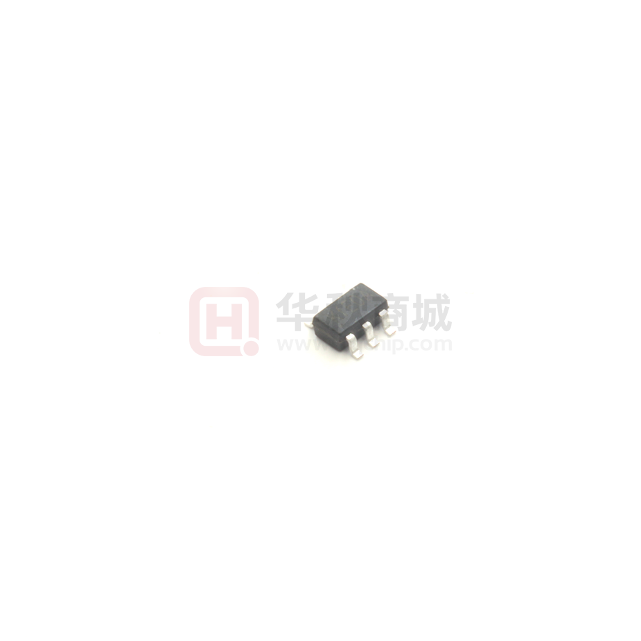
Available in SOT23-5 package
•
White-LED Supply for LCD Backlights
•
PDAs, Organizers, and Handheld PCs
Applications
•
•
LCD Bias Supply
Digital still cameras
General Description
The RY3751 is a high-frequency boost converter dedicated for small to medium LCD bias supply. The device is
ideal to generate output voltages up to 40V from a dual-cell NiMH/NiCd or a single-cell Li-Ion battery. The part
can also be used to generate standard 3.3V or 5V to 12V power conversions. Optimized operation frequency can
meet the requirement of small LC filters value and low operation current with high efficiency. Internal soft start
function can reduce the inrush current. The device has a 0.6A switch current limit, offering lower output voltage
ripple and allows the use of a smaller form factor inductor for lower power applications. Low quiescent current
allows device operation at very high efficiencies over the entire load current range. The RY3751 is available in
SOT23-5 package.
Typical Application Circuit
D2
C3
C4
D1
L1
VIN
D3
V2
-Voltage
V1
+Voltage
CIN
VIN
ON/
OFF
SW
R1
COUT
FB
R2
EN
GND
Typical Positive and Negative Output LCD Bias Supply Circuit
Email: support@rychip.com
©RYCHIP Semiconductor Inc.
http://www.rychip.com
Page 1 / 10
�RY3751
High Performance, 40V Output, 1MHz Bias Driver
Package and Pin Description
Pin Configuration
TOP VIEW
SW
1
GND
2
FB
3
5
IN
4
EN
SOT23-5
Pin Description
Pin
Name
Function
1
SW
Power Switch Output. SW is the drain of the internal MOSFET switch. Connect the
power inductor and output rectifier to SW. SW can swing between GND and 40V.
2
GND
3
FB
Feedback Input. The FB voltage is 1.23V. Connect a resistor divider to FB.
4
EN
EN pin of the boost converter. It is a multi-functional pin which can be used for
enable control and PWM dimming. Should not be left floating.
5
IN
Input Supply Pin. Must be locally bypassed.
Ground Pin.
Order Information (1)
Marking
KfYLL
Part No.
70390105
Model
RY3751AT5
Description
Package
T/R Qty
RY3751AT5 Bias Driver, VIN 2.5-5.5V,
VOUT VIN-40V, 1MHz, VFB1.23V,
SOT23-5
SOT23-5
3000PCS
Note (1): All RYCHIP parts are Pb-Free and adhere to the RoHS directive.
Email: support@rychip.com
©RYCHIP Semiconductor Inc.
http://www.rychip.com
Page 2 / 10
�RY3751
High Performance, 40V Output, 1MHz Bias Driver
Specifications
Absolute Maximum Ratings (1) (2)
Item
Min
Max
Unit
VIN, VEN voltage
-0.3
6
V
VSW voltage
-0.3
42
V
VSW voltage (10ns transient)
-5
43
V
All Other Pins
–0.3
6
V
Power dissipation
(3)
Internally Limited
Operating junction temperature, TJ
-40
150
°C
Storage temperature, Tstg
–65
150
°C
260
°C
Lead Temperature (Soldering, 10sec.)
Note (1): Exceeding these ratings may damage the device.
Note (2): The device is not guaranteed to function outside of its operating conditions.
Note (3): The maximum allowable power dissipation is a function of the maximum junction temperature, TJ(MAX),
the junction-to-ambient thermal resistance, RθJA, and the ambient temperature, TA. The maximum allowable power
dissipation at any ambient temperature is calculated using: PD (MAX) = (TJ(MAX) − TA)/RθJA. Exceeding the maximum
allowable power dissipation causes excessive die temperature, and the regulator goes into thermal shutdown.
Internal thermal shutdown circuitry protects the device from permanent damage. Thermal shutdown engages at
TJ=160°C (typical) and disengages at TJ= 130°C (typical).
ESD Ratings
Item
Description
Value
Unit
V(ESD-HBM)
Human Body Model (HBM)
ANSI/ESDA/JEDEC JS-001-2014
Classification, Class: 2
±2000
V
V(ESD-CDM)
Charged Device Mode (CDM)
ANSI/ESDA/JEDEC JS-002-2014
Classification, Class: C0b
±200
V
ILATCH-UP
JEDEC STANDARD NO.78E APRIL 2016
Temperature Classification,
Class: I
±150
mA
Min
Max
Unit
–40
125
°C
Operating temperature range
-40
85
°C
Input voltage VIN
2.5
5.5
V
Output voltage VOUT
VIN
38
V
Recommended Operating Conditions
Item
Operating junction temperature
(1)
Note (1): All limits specified at room temperature (TA = 25°C) unless otherwise specified. All room temperature
limits are 100% production tested. All limits at temperature extremes are ensured through correlation using standard
Statistical Quality Control (SQC) methods. All limits are used to calculate Average Outgoing Quality Level (AOQL).
Email: support@rychip.com
©RYCHIP Semiconductor Inc.
http://www.rychip.com
Page 3 / 10
�RY3751
High Performance, 40V Output, 1MHz Bias Driver
Thermal Information
Item
Description
(1)(2)
Value
Unit
180
°C/W
RθJA
Junction-to-ambient thermal resistance
RθJC(top)
Junction-to-case (top) thermal resistance
130
°C/W
RθJB
Junction-to-board thermal resistance
45
°C/W
ψJT
Junction-to-top characterization parameter
35
°C/W
ψJB
Junction-to-board characterization parameter
45
°C/W
Note (1): The package thermal impedance is calculated in accordance to JESD 51-7.
Note (2): Thermal Resistances were simulated on a 4-layer, JEDEC board
Electrical Characteristics (1) (2)
VIN=5V, TA=25°C, unless otherwise specified.
Parameter
Test Conditions
Min
Typ.
Max
Unit
Input voltage range
2.5
5.5
V
Output voltage range
VIN
38
V
Supply Current (Quiescent)
VFB =110%
150
300
µA
Supply Current (Shutdown)
VEN =0 or EN = GND
0.1
1
µA
1.23
1.26
V
SW On Resistance
400
650
mΩ
Current Limit
0.6
A
Output Over Voltage Protection
Threshold
40
V
Switching Frequency
1
MHz
90
%
80
ns
Feedback Voltage
Maximum Duty Cycle
1.20
VFB=90%
Minimum On-Time
EN Rising Threshold
1.2
V
EN Falling Threshold
Wake up VIN Voltage
Under-Voltage Lockout Threshold
Shutdown VIN Voltage
2.1
V
2.3
V
1.9
V
300
mV
Soft Start
600
µS
Thermal Shutdown
160
℃
Thermal Hysteresis
30
℃
Hysteresis VIN voltage
1.7
0.7
Note (1): MOSFET on-resistance specifications are guaranteed by correlation to wafer level measurements.
Note (2): Thermal shutdown specifications are guaranteed by correlation to the design and characteristics analysis.
Email: support@rychip.com
©RYCHIP Semiconductor Inc.
http://www.rychip.com
Page 4 / 10
�RY3751
High Performance, 40V Output, 1MHz Bias Driver
Typical Performance Characteristics (1) (2)
Note (1): Performance waveforms are tested on the evaluation board.
Note (2): VIN =5V, VOUT=12V, TA = +25ºC, unless otherwise noted.
Efficiency vs. Load Current
Load Regulation
Efficiency vs. Load Current
VOUT=12V
VOUT=12V
VOUT=12V/18V/24V
Load Regulation
Output Ripple Voltage
Output Ripple Voltage
VOUT=12V/18V/24V
VIN=5V, VOUT=12V, IOUT=100mA
VIN=5V, VOUT=12V, IOUT=200mA
Enable Startup at No Load
Enable Shutdown at No Load
Enable Startup at Heavy Load
VIN=5V, VOUT=12V
VIN=5V, VOUT=12V
VIN=5V, VOUT=12V, IOUT=200mA
Enable Shutdown at Heavy Load
Power Up at No Load
Power Up at Heavy Load
VIN=5V, VOUT=12V, IOUT=200mA
VIN=5V, VOUT=12V, IOUT=0A
VIN=5V, VOUT=12V, IOUT=200mA
Email: support@rychip.com
©RYCHIP Semiconductor Inc.
http://www.rychip.com
Page 5 / 10
�RY3751
High Performance, 40V Output, 1MHz Bias Driver
Functional Block Diagram
1MHz OSC
VIN
Current Bias
BandGap
ibias
OCP
600mA
PWM
Logic
VREF
SW
Buffer
Protection Circuit
FB
OVP
EN
UVLO
VREF
Soft Start
GND
Block Diagram
Functions Description
Under-Voltage Lockout (UVLO)
Under-voltage lockout (UVLO) protects the chip from operating at an insufficient supply voltage. UVLO protection
monitors the internal regulator voltage. When the voltage is lower than UVLO threshold voltage, the device is shut
off. When the voltage is higher than UVLO threshold voltage, the device is enabled again.
Enable and Disable
When the input voltage is above maximal UVLO rising threshold and the EN pin is pulled high, the RY3751 is
enabled. When the EN pin is pulled low, the RY3751 goes into shutdown mode. In shutdown mode, less than 1μA
input current is consumed. Because there is a conductive path from the input to the output through the inductor and
Schottky diode, the output voltage is equal to the input voltage during shutdown. The enable pin needs to be
terminated and should not be left floating.
Soft-Start
All inductive step-up converters exhibit high inrush current during start-up if no special precaution is made. This
can cause voltage drops at the input rail during start up and may result in an unwanted or early system shut down.
An internal soft start circuit limits the peak inductor current according to the output voltage. The switching soft start
phase is about 600µs typically. The soft start function reduces the inrush current during startup.
Email: support@rychip.com
©RYCHIP Semiconductor Inc.
http://www.rychip.com
Page 6 / 10
�RY3751
High Performance, 40V Output, 1MHz Bias Driver
Over-Voltage Protection
As with any current source, the output voltage rises when the output gets high impedance or disconnected. To
prevent the output voltage exceeding the maximum switch voltage rating of the main switch, an overvoltage
protection circuit is integrated. As soon as the output voltage exceeds the OVP threshold, the converter stops
switching and the output voltage falls.
Thermal Shutdown
Thermal shutdown prevents the chip from operating at exceedingly high temperatures. When the silicon die
temperature exceeds 160°C, it shuts down the whole chip. When the temperature falls below its lower threshold
(Typ. 130°C) the chip is enabled again.
Applications Information
Typical Application
V2
-18V
D3
C3
1µF
L1=10µH
VIN
CIN
4.7µF
VIN
ON/
OFF
SW
FB
EN
GND
D2
C4
44µF
V1
18V
D1
R1
136K
COUT
44µF
R2
10K
Positive and Negative Output LCD Bias Supply Circuit
L1=10µH
VIN
CIN
4.7µF
VIN
ON/
OFF
SW
D1
R1
136K
VOUT
18V
COUT
44µF
FB
EN
GND
R2
10K
Boost Application Circuit
Email: support@rychip.com
©RYCHIP Semiconductor Inc.
http://www.rychip.com
Page 7 / 10
�RY3751
High Performance, 40V Output, 1MHz Bias Driver
Setting the Output Voltage
The output voltage can be programmed by resistor divider, as shown in Equation:
Inductor Selection
𝑉𝑉𝑂𝑂𝑂𝑂𝑂𝑂 = 1.23𝑉𝑉 × (1 +
𝑅𝑅1
)
𝑅𝑅2
The recommended value of inductor for most applications are 4.7 to 22μH. Small size and better efficiency are the
major concerns for portable device, such as RY3751 used for mobile phone. When selecting the inductor, the inductor
saturation current should be rated as high as the peak inductor current at maximum load, and respectively, maximum
LED current.
The inductor value determines the maximum switching frequency of the converter. Therefore, select the inductor
value that ensures the maximum switching frequency at the converter maximum load current is not exceeded. The
maximum switching frequency is calculated by the following formula:
𝑉𝑉𝐼𝐼𝐼𝐼(𝑚𝑚𝑚𝑚𝑚𝑚) × (𝑉𝑉𝑂𝑂𝑂𝑂𝑂𝑂 − 𝑉𝑉𝐼𝐼𝐼𝐼 )
𝑓𝑓𝑆𝑆(𝑀𝑀𝑀𝑀𝑀𝑀) =
𝐼𝐼𝑃𝑃 × 𝐿𝐿 × 𝑉𝑉𝑂𝑂𝑂𝑂𝑂𝑂
Where:
IP = Peak current.
L = Selected inductor value.
VIN (min) = The highest switching frequency occurs at the minimum input voltage.
If the selected inductor value does not exceed the maximum switching frequency of the converter, the next step is
to calculate the switching frequency at the nominal load current using the following formula:
2 × 𝐼𝐼𝑙𝑙𝑙𝑙𝑙𝑙𝑙𝑙 × (𝑉𝑉𝑂𝑂𝑂𝑂𝑂𝑂 − 𝑉𝑉𝐼𝐼𝐼𝐼 + 𝑉𝑉𝑑𝑑 )
𝑓𝑓𝑆𝑆 (𝐼𝐼𝑙𝑙𝑙𝑙𝑙𝑙𝑙𝑙 ) =
𝐼𝐼𝑃𝑃2 × 𝐿𝐿
Where:
IP = Peak current.
L = Selected inductor value.
Iload=Nominal load current.
Vd= Rectifier diode forward voltage.
A smaller inductor value gives a higher converter switching frequency, but lowers the efficiency.
The inductor value has less effect on the maximum available load current and is only of secondary order. The best
way to calculate the maximum available load current under certain operating conditions is to estimate the expected
converter efficiency at the maximum load current.
𝐼𝐼𝑙𝑙𝑙𝑙𝑙𝑙𝑙𝑙(𝑚𝑚𝑚𝑚𝑚𝑚) = 𝜂𝜂
𝐼𝐼𝑃𝑃2 × 𝐿𝐿 × 𝑓𝑓𝑠𝑠(𝑚𝑚𝑚𝑚𝑚𝑚)
2 × (𝑉𝑉𝑂𝑂𝑂𝑂𝑂𝑂 − 𝑉𝑉𝐼𝐼𝐼𝐼 )
Where:
IP = Peak current.
L = Selected inductor value.
fSmax= Maximum switching frequency as calculated previously.
η = Expected converter efficiency.
The selected inductor should have a saturation current that meets the maximum peak current of the converter.
Another important inductor parameter is the dc resistance. The lower the dc resistance, the higher the efficiency of
the converter.
Email: support@rychip.com
©RYCHIP Semiconductor Inc.
http://www.rychip.com
Page 8 / 10
�RY3751
High Performance, 40V Output, 1MHz Bias Driver
Output Capacitor Selection
The device is designed to operate with a wide selection of ceramic output capacitors. The selection of the output
capacitor value is a trade-off between output voltage ripple and capacitor cost and form factor. In general, capacitor
values of 10µF up to 44µF can be used. For better voltage filtering, ceramic capacitors with low ESR are recommended.
X5R and X7R types are suitable because of their wider voltage and temperature ranges.
Input Capacitor Selection
For good input voltage filtering, low ESR ceramic capacitors are recommended. A 4.7µF ceramic input capacitor is
sufficient for most of the applications. For better input voltage filtering and EMI reduction, this value can be
increased. The input capacitor should be placed as close as possible to the input pin of the converter.
Diode Selection
A Schottky diode should be used for the output diode. The forward current rating of the diode should be higher than
the load current, and the reverse voltage rating must be higher than the output voltage. Do not use ordinary rectifier
diodes, since slow switching speeds and long recovery times cause the efficiency and the load regulation to suffer.
Layout Guidelines
For best performance of the RY3751, the following guidelines must be strictly followed.
1. Input and Output capacitors should be placed close to the IC and connected to ground plane to reduce noise
coupling.
2. The GND should be connected to a strong ground plane for heat sinking and noise protection.
3. Keep the main current traces as possible as short and wide.
4. SW node of DC-DC converter is with high frequency voltage swing. It should be kept at a small area.
5. Place the feedback components as close as possible to the IC and keep away from the noisy devices.
Top Layer
Bottom Layer
Sample Board Layout
Email: support@rychip.com
©RYCHIP Semiconductor Inc.
http://www.rychip.com
Page 9 / 10
�RY3751
High Performance, 40V Output, 1MHz Bias Driver
Package Description
SOT23-5
2.80
3.00
0.95
BSC
0.60
TYP
1.20
TYP
EXAMPLE
TOP MARK
AAAAA
1.50
2.60
1.70
3.00
2.60
TYP
PIN 1
TOP VIEW
RECOMMENDED PAD LAYOUT
GAUGE PLANE
0.25 BSC
0.90
1.30
1.45 MAX
SEATING PLANE
0.30
0.50
0.95 BSC
FRONT VIEW
0.00
0.15
0° ~8°
0.30
0.55
0.09
0.20
SIDE VIEW
NOTE:
1. CONTROL DIMENSION IS IN INCHES. DIMENSION IN BRACKET IS IN MILLIMETERS.
2. PACKAGE LENGTH DOES NOT INCLUDE MOLD FLASH, PROTRUSIONS OR GATE BURRS.
3. PACKAGE WIDTH DOES NOT INCLUDE INTERLEAD FLASH OR PROTRUSIONS.
4. LEAD COPLANARITY (BOTTOM OF LEADS AFTER FORMING) SHALL BE 0.004" INCHES MAX.
5. DRAWING CONFORMS TO JEDEC MS-012, VARIATION BA.
6. DRAWING IS NOT TO SCALE.
Email: support@rychip.com
©RYCHIP Semiconductor Inc.
http://www.rychip.com
Page 10 / 10
�