SD12T1G
Features
Description
* 400W peak pulse power (8/20μs)
* Protects one data or power line
* Ultra low leakage: nA level
* Operating voltage: 12V
* Ultra low clamping voltage
The SD12T1G is designed to replace multilayer
varistors in portable applications such as cell
phones, notebook computers and PDA’s, using
monolithic
sili-con
technology
to
provide
fast
response time and ultra low ESD clamping voltage,
* Complies with following standards:
making this device an ideal solution for protecting
– IEC 61000-4-2 (ESD) immunity test
sensitive semiconductor compo-nents from damage.
Air discharge: ±30kV
Contact discharge: ±30kV
– IEC61000-4-4 (Lightning) 18A (8/20ns)
The SD12T1G complies with the IEC 61000-4-2
(ESD) standard with ±15kV air and ±8kV contact
discharge. The SD12T1G is assembled into a lead-free
SOD-323 package and will protect one unidirectional
RoHS Compliant
line. These devices will fit on the same PCB pad area
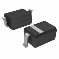
Package: SOD-323
as an 0805 MLV device.
Lead Finish: Matte Tin
Circuit Diagram
Marking Diagram
5Y
Applications
Cellular Handsets and Accessories
Personal Digital Assistants
Notebooks and Handhelds
Portable Instrumentation
Peripherals
Pagers Peripherals
Desktop and Servers
Ordering Information
Part Number
Packaging
Reel Size
SD12T1G
3000/Tape & Reel
7 inch
Transparent top view
12B:Device Marking Code
Ver.: A1 2019-02-22 AW
0571-87006810
www.dowosemi.cn
1/4
�SD12T1G
Absolute Maximum Ratings (TA=25°C unless otherwise specified)
Parameter
Symbol
Value
Unit
Peak Pulse Power (8/20µs)
Ppk
400
W
Peak Pulse Current (8/20µs)
IPP
18
A
ESD per IEC 61000−4−2 (Air)
±30
VESD
ESD per IEC 61000−4−2 (Contact)
Operating Temperature Range
Storage Temperature Range
kV
±30
TJ
−55 to +125
°C
Tstg
−55 to +150
°C
Electrical Characteristics (TA=25°C unless otherwise specified)
Parameter
Symbol
Reverse Working Voltage
Breakdown Voltage
Test Condition
Min
Typ
VRWM
VBR
IT = 1mA
13.0
14.0
Max Unit
12.0
V
16.0
V
0.5
µA
Reverse Leakage Current
IR
VRWM = 12.0V
Clamping Voltage
VC
IPP = 1A (8 x 20µs pulse)
17
19
V
Clamping Voltage
VC
IPP = 18A (8 x 20µs pulse)
20
25
V
Junction Capacitance
CJ
VR = 0V, f = 1MHz
15
30
pF
Portion Electronics Parameter
Symbol
IT
IPP
Vc
Parameter
Test Current
Maximum Reverse Peak Pulse Current
Clamping Voltage @Ic
Ver.: A1 2019-02-22 AW
0571-87006810
www.dowosemi.cn
2/4
�SD12T1G
Typical Performance Characteristics (TA=25°C unless otherwise Specified)
20
15
10
5
0
28
Vc-Clamping Voltage(V)
CJ-Junction Capacitance (pF)
25
0
2
4
6
8
10
24
20
16
12
8
4
0
12
0
2
VR—Reverse Voltage(V)
4
6
8
10
12
14
16
18
20
Ipp-Peak Pulse Current(A)
Clamping Voltage vs. Peak Pulse Current
Junction Capacitance vs. Reverse Voltage
Voltage (V)
Peak Power_Ppp(kW)
10
1
0.1
-20
0.1
1.0
10.0
Pulse Duration_tp(uS)
100
100
80
60
40
20
50
75
100
125
150
Ipp-Peak Pulse Current-%of Ipp
% of Rated Power
120
25
40
60
80
Ambient Temperature_Ta(℃)
80
60
40
20
0
-20
-20
0
20
40
T-Time(us)
8 X 20us Pulse Waveform
Power Derating Curve
Ver.: A1 2019-02-22 AW
0571-87006810
100
IEC61000−4−2 Pulse Waveform
120
0
20
Time (nS)
Peak Pulse Power vs. Pulse Time
0
0
100.0
www.dowosemi.cn
3/4
60
�SD12T1G
SOD-323 Package Outline Drawing
DIMENSIONS
SYM
MILLIMETERS
INCHES
MIN
MAX
MIN
MAX
A
1.50
1.80
0.060
0.071
B
1.20
1.40
0.045
0.054
C
2.30
2.70
0.090
0.107
D
-
1.10
-
0.043
E
0.30
0.40
0.012
0.016
F
0.10
0.25
0.004
0.010
H
-
0.10
-
0.004
Suggested Land Pattern
SYM
DIMENSIONS
MILLIMETERS
INCHES
A
3.15
0.120
B
0.80
0.031
C
0.80
0.031
Ver.: A1 2019-02-22 AW
0571-87006810
www.dowosemi.cn
4/4
�
很抱歉,暂时无法提供与“SD12T1G”相匹配的价格&库存,您可以联系我们找货
免费人工找货- 国内价格
- 10+0.20146
- 100+0.19844
- 600+0.13078
- 1200+0.12882
- 国内价格
- 20+0.15596
- 200+0.11805
- 600+0.09699
- 3000+0.09623
- 9000+0.08532
- 21000+0.07938
- 国内价格
- 1+0.44220
- 200+0.14740
- 1500+0.09207
- 3000+0.07304