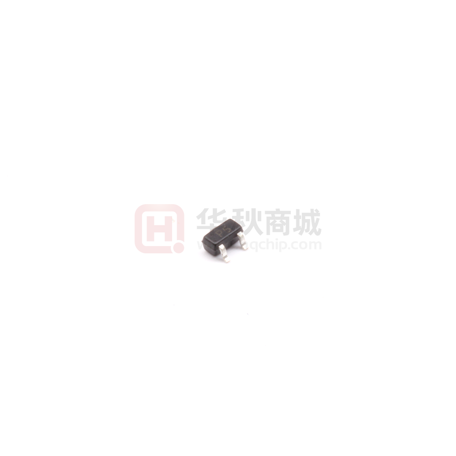
RCLAMP0502B
2-Line Ultra Low Capacitance TVS Diode
Features
Description
Ultra low capacitance: 0.3pF typical (I/O to I/O)
Ultra low leakage: nA level
Low operating voltage: 5V
Low clamping voltage
Up to 2 data lines protects
Package: SOT-523
Complies with following standards:
The RCLAMP0502B is an ultra low capacitance
TVS array, utilizing leading monolithic silicon technology to provide fast response time and low ESD
clamping voltage, making this device an ideal solution for protecting voltage sensitive high-speed data
lines. The RCLAMP0502B has very low capacitance
with a typical value at 0.3pF, and complies with the
IEC 61000-4-2 (ESD) standard with ±15kV air and
±8kV contact discharge. It is assembled into a 3-pin
lead-free SOT-523 package. The combination of
small size, low capacitance and high level of ESD
protection makes it ideal for HDMI, MDDI, antenna
circuits, USB 2.0.
– IEC 61000-4-2 (ESD) immunity test
Air discharge: ±15kV
Contact discharge: ±8kV
– IEC61000-4-4 (EFT) 40A (5/50ns)
IEC61000-4-5 (Lightning) 4A (8/20μs)
RoHS Compliant
Circuit Diagram
1
2
3
Applications
Smart phones
Display Ports
MDDI Ports
USB Ports
Digital Video Interface (DVI)
PCI Express and Serial SATA Ports
Marking Diagram
Ordering Information
3
Part Number
5B
1
Packaging
RCLAMP0502B 3000/Tape & Reel
2
Transparent top view
P5:Device Marking Code
1 of 4
Reel Size
7 inch
�RCLAMP0502B
Absolute Maximum Ratings (TA=25°C unless otherwise specified)
Parameter
Symbol
Value
Unit
Peak Pulse Power (8/20µs)
Ppk
70
W
Peak Pulse Current (8/20µs)
IPP
4
A
ESD per IEC 61000−4−2 (Air)
±20
VESD
ESD per IEC 61000−4−2 (Contact)
Operating Temperature Range
Storage Temperature Range
kV
±15
TJ
−55 to +125
°C
Tstg
−55 to +150
°C
Electrical Characteristics (TA=25°C unless otherwise specified)
Parameter
Symbol
Reverse Working Voltage
Breakdown Voltage
Test Condition
VBR
IR
Clamping Voltage
VC
Clamping Voltage
VC
Junction Capacitance
CJ
Junction Capacitance
CJ
IT = 1mA
6.0
VRWM = 5.0V
IPP = 1A (8 x 20µs pulse)
IPP = 4.0A (8 x 20µs pulse)
VR = 0V, f = 1MHz,pin 1 or
pin 2 to pin 3
VR = 0V, f = 1MHz,between
pin 1 and pin 2
Portion Electronics Parameter
IT
IPP
Vc
Typ
VRWM
Reverse Leakage Current
Symbol
Min
Parameter
Test Current
Maximum Reverse Peak Pulse Current
Clamping Voltage @Ic
2 of 4
Max Unit
5.0
V
8.5
V
0.5
µA
9
11
V
13
15
V
0.6
1.0
pF
0.3
0.5
pF
7.5
�RCLAMP0502B
Typical Performance Characteristics (TA=25°C unless otherwise Specified)
20
Vc-Clamping Voltage(V)
CJ-Junction Capacitance (pF)
1
0.9
0.8
0.7
0.6
0.5
0.4
0.3
0.2
16
12
8
4
0.1
0
0
0
1
2
3
4
0
5
1
VR—Reverse Voltage(V)
2
3
4
5
Ipp-Peak Pulse Current(A)
Clamping Voltage vs. Peak Pulse Current
Junction Capacitance vs. Reverse Voltage
1
Voltage (V)
Peak Power_Ppp(kW)
10
0.1
0.01
0.1
1
10
-20
100
0
20
120
120
100
100
80
60
40
20
0
50
75
100
125
80
100
IEC61000−4−2 Pulse Waveform
Ipp-Peak Pulse Current-%of Ipp
% of Rated Power
Peak Pulse Power vs. Pulse Time
25
60
Time (nS)
Pulse Duration_tp(uS)
0
40
150
80
60
40
20
0
-20
-20
Ambient Temperature_Ta(℃)
0
20
40
T-Time(us)
8 X 20us Pulse Waveform
Power Derating Curve
3 of 4
60
�RCLAMP0502B
SOT-523 Package Outline Drawing
Suggested Land Pattern
4 of 4
�
很抱歉,暂时无法提供与“RCLAMP0502B”相匹配的价格&库存,您可以联系我们找货
免费人工找货- 国内价格
- 10+0.27994
- 100+0.22292
- 300+0.19440
- 3000+0.15876
- 6000+0.14170
- 9000+0.13306
- 国内价格
- 1+0.25740
- 200+0.16610
- 1500+0.14410
- 3000+0.12760
- 国内价格
- 10+0.24365
- 100+0.19402
- 600+0.16920
- 1200+0.16666
- 3000+0.13818
