Preliminary Datasheet
LP5300
Over Voltage and Over Current Protection IC
General Description
Features
The LP5300 is an Over-Voltage-Protection (OVP) and
Input Voltage Range: 3V to 36V
Over-Current-Protection (OCP) device. The device will
Typical Output Power on Time: 9ms
switch off internal MOSFET to disconnect VIN to
OVP Threshold: 6.1V
OVP Threshold Time Less Than 1μs
Over Current Protection: 2.1A(MIN)
Low RDS(ON) Internal Switches:130mΩ @ 5V /1A
Output Discharge
Thermal Fault Protection
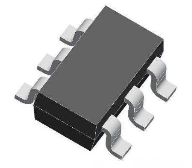
SOT23-6/SOT89 Package
RoHS Compliant and 100% Lead (Pb)-Free
VOUT to protect load when any of input voltage, input
current over the threshold. The Over temperature
protection (OTP) function monitors chip temperature to
protect the device.
The LP5300 is available in SOT-23-6L and SOT89
package.
Standard
products
are
Halogen-free.
Pb-free
and
Order Information
Typical Application Circuit
LP5300 □ □ □
F: Pb-Free
VIN
OUT
LP5300
VIN
Package Type
B6:SOT23-6
VOUT
C2
1uF
C1
1uF
GND
X3:SOT89
Applications
GPS
PMP
PAD
MID
Digital cameras, Digital Videos
Marking Information
Device
Marking
Package
Shipping
LP5300B6F
8WYWX
SOT23-6
3K/REEL
LP5300X3F
LPS
SOT89
1K/REEL
LP5300
YWX
Marking indication:
Y:Production year W:Production week
LP5300-02
Oct.-2015
Email: marketing@lowpowersemi.com
X:Production batch
www.lowpowersemi.com
Page 1 of 7
�Preliminary Datasheet
LP5300
Functional Pin Description
Top View
GND
1
6
GND
GND
2
5
GND
VIN
3
4
VOUT
SOT23-6
1
2
VOUT
GND
3
VIN
SOT89
Pin Description
Pin
SOT23-6
SOT89
1,2,5,6
2
Name
Description
GND
Ground.
Input pin. A 1uF low ESR ceramic capacitor or larger must be connected as
3
3
VIN
close as to this pin. It is recommended to use 50V capacitor or according to
application.
4
LP5300-02
1
VOUT
Oct.-2015
Output pin.
Email: marketing@lowpowersemi.com
www.lowpowersemi.com
Page 2 of 7
�Preliminary Datasheet
LP5300
Function Diagram
Absolute Maximum Ratings Note 1
Input Voltage to GND ---------------------------------------------------------------------------------------------------- 36V
Output Voltage to GND ------------------------------------------------------------------------------------------------ 6.5V
Maximum Junction Temperature ---------------------------------------------------------------------------------- 150℃
Operating Ambient Temperature Range (TA) -------------------------------------------------------- -40℃ to 85℃
Maximum Soldering Temperature (at leads, 10 sec) -------------------------------------------------------- 260℃
Note 1.
Stresses beyond those listed under “Absolute Maximum Ratings” may cause permanent damage to the device. These are stress
ratings only, and functional operation of the device at these or any other conditions beyond those indicated in the operational
sections of the specifications is not implied. Exposure to absolute maximum rating conditions for extended periods may affect
device reliability.
Thermal Information
Maximum Power Dissipation (SOT23-6, PD,TA=25℃) ------------------------------------------------------ 0.45W
Thermal Resistance (SOT23-6, θJA) ------------------------------------------------------------------------- 250℃/W
Maximum Power Dissipation (SOT89, PD,TA=25℃) ---------------------------------------------------------- 0.7W
Thermal Resistance (SOT89, θJA) ---------------------------------------------------------------------------- 165℃/W
ESD Susceptibility
HBM(Human Body Mode) --------------------------------------------------------------------------------------------- 2KV
MM(Machine Mode) --------------------------------------------------------------------------------------------------- 200V
LP5300-02
Oct.-2015
Email: marketing@lowpowersemi.com
www.lowpowersemi.com
Page 3 of 7
�Preliminary Datasheet
LP5300
Electrical Characteristics
TA=25℃, unless otherwise noted
Symbol
Parameter
Condition
Min
Typ
Max
Units
36
V
DC characteristics and Power-ON-Reset
VIN
Input Voltage
3
IQ
Input quiescent current
VIN=5V, IOUT=0A
80
μA
RON
VIN-to-VOUT ON resistance
VIN=5V, IOUT=1A
130
mΩ
RDISCHARGE
Output discharge resistance
3.6
KΩ
UVLO
Under voltage lock out threshold
VIN increasing from 0~3V
VHYS-UVLO
Under voltage lock out hysteresis
VIN decreasing from 3~0V
150
mV
TON
Output power-on time
VIN=0→5V to output ON
9
ms
2.6
2.8
3
V
Input Over-Voltage-Protection (OVP)
VOVP
OVP threshold
VIN increasing from 5~7V
VHYS-OVP
OVP hysteresis
VIN decreasing from 7~5V
TOVP
OVP active time
VIN=5→10V
TON(OVP)
OVP recovery time
VIN=10→5V to output ON
5.8
6.1
6.4
300
V
mV
1
μs
9
ms
2.5
A
Input Over-Current-Protection (OCP)
IOCP
OCP threshold
2.1
tOCP
OCP active time
30
ms
tON(OCP)
OCP recovery time
1
s
Over-Temperature-Protection (OTP)
TOTP
OTP threshold
150
℃
TOTP_HYS
OTP hysteresis
20
℃
LP5300-02
Oct.-2015
Email: marketing@lowpowersemi.com
www.lowpowersemi.com
Page 4 of 7
�Preliminary Datasheet
LP5300
Typical Operating Characteristics
OVP waveform
LP5300-02
Oct.-2015
Email: marketing@lowpowersemi.com
VIN falling waveform
www.lowpowersemi.com
Page 5 of 7
�Preliminary Datasheet
LP5300
Packaging Information
SOT23-6
LP5300-02
Oct.-2015
Email: marketing@lowpowersemi.com
www.lowpowersemi.com
Page 6 of 7
�Preliminary Datasheet
LP5300
SOT89
LP5300-02
Oct.-2015
Email: marketing@lowpowersemi.com
www.lowpowersemi.com
Page 7 of 7
�
很抱歉,暂时无法提供与“LP5300B6F”相匹配的价格&库存,您可以联系我们找货
免费人工找货- 国内价格
- 5+0.88377
- 50+0.70233
- 150+0.61161
- 500+0.54357
- 3000+0.48536
- 6000+0.45814
- 国内价格
- 1+0.68860
- 200+0.47520
- 1500+0.43230
- 3000+0.40370
- 国内价格
- 10+0.54095
- 100+0.50605
- 500+0.47115
- 2000+0.41880
- 5000+0.40135
- 10000+0.39088