LAD8C05L01
Electrostatic Discharged Protection Devices (ESD) Data Sheet
Description
The LAD8C05L01 of Transient Voltage Suppressors are designed
to replace multilayer varistors (MLVs) in portable applications such
as cell phones, notebook computer, and PDAs.
They offer superior electrical characteristics such as lower clamping
voltage and no device degradation when compared to MLVs. They
are designed to protect sensitive semiconductor components from
damage or upset due to electrostatic discharge (ESD), lightning,
electrical fast transients (EFT), and cable discharge events (CDE).
Features
●
●
●
●
●
●
●
●
●
●
●
IEC61000-4-2 ESD 15KV Air, 8KV contact compliance
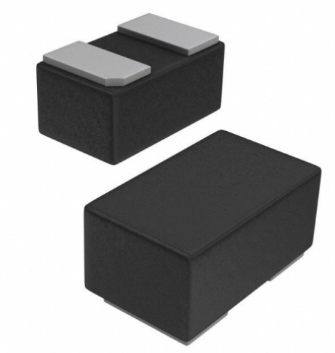
SOD882 surface mount package
Working voltage: 5V
Low leakage current
Low operating and clamping voltages
Solid-state silicon avalanche technology
RoHS compliant
Solder reflow temperature: Pure Tin-Sn, 260~270℃
Flammability rating UL 94V-0
Meets MSL level 1, per J-STD-020
Marking: BB
1
2
Pin Configuration
Applications
● Cellular Handsets & Accessories
● Notebooks & Handhelds
● Digital Cameras
● Personal Digital Assistants (PDAs)
● Portable Instrumentation
Maximum Ratings
Rating
Peak Pulse Current(tp=8/20μs)
Symbol
Value
Unit
IPP
4
A
ESD voltage (Contact discharge)
±8
VESD
ESD voltage (Air discharge)
Storage & operating temperature range
Revision: ESD-LAD8C05L01-001(A1)
kV
±15
TSTG ,TJ
1/4
-55~+150
℃
http://brightking.pulseelectronics.com
�LAD8C05L01
Electrical Characteristics (TJ=25℃)
Parameter
Symbol
Reverse stand-off voltage
Condition
Min.
Typ.
VRWM
Reverse breakdown voltage
Max.
Unit
5
V
VBR
IBR=1mA
5.5
V
Reverse leakage current
IR
VR=5V
1
μA
Clamping voltage (tp=8/20μs)
VC
IPP=1A
8.5
V
Clamping voltage (tp=8/20μs)
VC
IPP=4A
12
V
Off state junction capacitance
CJ
0Vdc,f=1MHz
10
pF
Typical Characteristics Curves
Figure 1. Pulse Waveforms
tr
25
Peak value Ipp
Waveform
Parameters:
tr=8µs
td=20µs
90
80
Clamping Voltage (V)
% of Peak Power Current
110
100
Figure 2. Clamping Voltage vs. Peak Pulse Current
70
60
50
40
30
td=t|IPP/2
20
20
15
10
Waveform
Parameters:
tr=8µs
tb=20µs
5
10
0
0
0
5
10
15
20
25
30
t-Time (μs)
0
1
2
3
4
5
6
IPP-Peak Pulse Current (A)
Figure 3. Capacitance vs. Reverse Voltage
25
Junction Capacitance (pF)
F=1MHz
20
15
10
5
0
0
1
2
3
4
5
Reverse Voltage (V)
Revision: ESD-LAD8C05L01-001(A1)
2/4
http://brightking.pulseelectronics.com
�LAD8C05L01
Recommended Soldering Conditions
Reflow Soldering
Critical Zone
TL to TP
tP
TP
Ramp-up
TL
tL
Temperature
TS max
TS min
Ramp-down
tS
Preheat
25
t 25℃ to Peak
Time
Recommended Conditions
Profile Feature
Pb-Free Assembly
Average ramp-up rate (TL to TP)
3℃/second max.
Preheat
-Temperature Min (TS min)
-Temperature Max (TS max)
-Time (min to max) (ts)
150℃
200℃
60-180 seconds
TS max to TL
-Ramp-up Rate
3℃/second max.
Time maintained above:
-Temperature (TL)
-Time (tL)
217℃
60-150 seconds
Peak Temperature (TP)
260℃
Time within 5℃ of actual Peak Temperature (tP)
Ramp-down Rate
6℃/second max.
Time 25℃ to Peak Temperature
Revision: ESD-LAD8C05L01-001(A1)
20-40 seconds
8 minutes max.
3/4
http://brightking.pulseelectronics.com
�LAD8C05L01
Dimensions (SOD882)
Dimension (mm)
A
Symbol
B
C
Side View
Top View
D
E
0.30
0.60
0.05
Recommended Soldering Pad Layout
Bottom View
Min.
Max.
Min.
Max.
A
0.95
1.05
0.037
0.041
B
0.55
0.65
0.022
0.026
C
0.32
0.55
0.013
0.022
D
1.40
0.125
Inches
0.55
F
45°
Millimeters
0.45
0.018
E
0.20
0.30
0.008
0.012
F
0.45
0.55
0.018
0.022
Packaging
Tape
P0
P1
P2
K
B
W
F
E
øD0
øD1
t
A
Reel
D2
D
Revision: ESD-LAD8C05L01-001(A1)
W1
4/4
Symbol
Dimension (mm)
W
8.00±0.30
P0
4.00±0.10
P1
2.00±0.10
P2
2.00±0.10
D0
Φ1.55±0.10
D1
Φ0.40±0.05
E
1.75±0.10
F
3.50±0.10
A
0.75±0.10
B
1.15±0.10
K
0.60±0.05
t
0.20±0.05
D
Φ328.0±2.0
D2
Φ14.4
W1
10.0
Quantity: 40000PCS
http://brightking.pulseelectronics.com
�
很抱歉,暂时无法提供与“LAD8C05L01”相匹配的价格&库存,您可以联系我们找货
免费人工找货- 国内价格
- 20000+0.15120
- 40000+0.10960
- 200000+0.09870
- 国内价格
- 50+0.09000
- 500+0.08100
- 5000+0.07500
- 10000+0.07200
- 30000+0.06900
- 50000+0.06720