Plastic-Encapsulate MOSFETS
P-Channel 20-V(D-S) MOSFET SOT-23
FEATURE
TrenchFET Power MOSFET
1. GATE
2. SOURCE
3. DRAIN
APPLICATIONS
z
Load Switch for Portable Devices
z
DC/DC Converter
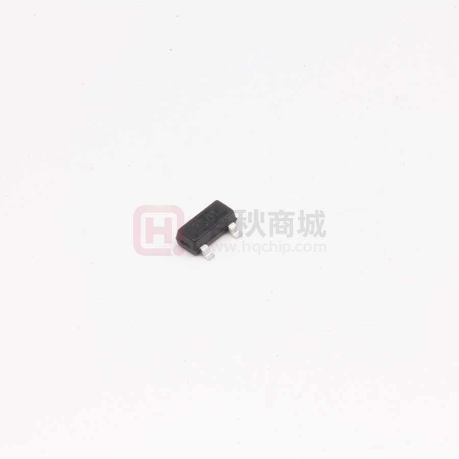
MARKING: 2301
Maximum ratings (Ta=25℃ unless otherwise noted)
Parameter
Symbol
Value
Drain-Source Voltage
VDS
-20
Gate-Source Voltage
VGS
±8
Continuous Drain Current
ID
-2.3
Pulsed Drain Current
IDM
-10
Continuous Source-Drain Diode Current
IS
-0.72
Maximum Power Dissipation
PD
0.35
W
R θJA
357
℃/W
Junction Temperature
TJ
150
Storage Temperature
Tstg
-55 ~+150
Thermal Resistance from Junction to Ambient(t ≤5s)
Unit
V
A
℃
1 of 4
Copyright © All right reserved: Heyuan China Base Electronics Technology Co., Ltd.
�Electrical characteristics (Ta=25℃ unless otherwise noted)
Parameter
Symbol
Test Condition
Min
Typ
Max
Units
Static
Drain-source breakdown voltage
V(BR)DSS
VGS = 0V, ID =-250µA
-20
Gate-source threshold voltage
VGS(th)
VDS =VGS, ID =-250µA
-0.4
V
-1
Gate-source leakage
IGSS
VDS =0V, VGS =±8V
±100
nA
Zero gate voltage drain current
IDSS
VDS =-20V, VGS =0V
-1
µA
Drain-source on-state resistance a
Forward transconductance
RDS(on)
a
gfs
VGS =-4.5V, ID =-2.8A
0.090
0.112
VGS =-2.5V, ID =-2.0A
0.110
0.142
VDS =-5V, ID =-2.8A
6.5
Ω
S
b
Dynamic
Input capacitance
Ciss
Output capacitance
Coss
Reverse transfer capacitance
Crss
Total gate charge
Qg
Gate-source charge
Qgs
Gate-drain charge
Qgd
Gate resistance
Rg
Turn-on delay time
405
VDS =-10V,VGS =0V,f =1MHz
55
VDS =-10V,VGS =-4.5V,ID =-3A
VDS =-10V,VGS =-2.5V,ID =-3A
tr
Turn-off delay time
td(off)
Fall time
5.5
10
3.3
6
nC
0.7
1.3
f =1MHz
td(on)
Rise time
pF
75
VDD=-10V,
RL=10Ω, ID =-1A,
VGEN=-4.5V,Rg=1Ω
tf
Ω
6.0
11
20
35
60
30
50
10
20
ns
Drain-source body diode characteristics
Continuous source-drain diode current
Pulse diode forward current
Body diode voltage
a
IS
-1.3
TC=25℃
-10
ISM
VSD
A
IS=-0.7A
-0.8
-1.2
Notes :
a.Pulse Test : Pulse Width < 300µs, Duty Cycle ≤2%.
b.Guaranteed by design, not subject to production testing.
2 of 4
Copyright © All right reserved: Heyuan China Base Electronics Technology Co., Ltd.
V
�BC2301
Typical Characteristics
Output Characteristics
Transfer Characteristics
-14
-10
Ta=25℃
VGS= -4.0V,-3.5V,-3.0V,-2.5V
Ta=25℃
Pulsed
Pulsed
VGS=-2.0V
-12
-8
(A)
-6
VGS=-1.5V
-4
ID
-8
-6
DRAIN CURRENT
DRAIN CURRENT
ID
(A)
-10
-4
-2
-2
VGS=-1.0V
-0
-0
-1
-2
-3
DRAIN TO SOURCE VOLTAGE
RDS(ON)
VDS
-0
-0.0
-4
(V)
-1.0
ID
——
-1.5
GATE TO SOURCE VOLTAGE
RDS(ON)
——
-2.0
VGS
-2.5
(V)
VGS
250
150
Ta=25℃
Ta=25℃
Pulsed
Pulsed
200
(mΩ)
60
RDS(ON)
VGS=-2.5V
90
ON-RESISTANCE
RDS(ON)
(mΩ)
120
ON-RESISTANCE
-0.5
VGS=-4.5V
30
150
100
ID=-3.6A
50
0
0
-0
-2
-4
-6
DRAIN CURRENT
IS
——
ID
-8
-0
-10
(A)
-2
-4
GATE TO SOURCE VOLTAGE
-6
VGS
(V)
VSD
-1
Ta=25℃
Pulsed
-0.1
SOURCE CURRENT
IS
(A)
-0.3
-0.03
-0.01
-3E-3
-1E-3
-0.2
-0.4
-0.6
-0.8
SOURCE TO DRAIN VOLTAGE
-1.0
VSD
-1.2
(V)
3 of 4
Copyright © All right reserved: Heyuan China Base Electronics Technology Co., Ltd.
-8
�PACKAGE OUTLINE
Plastic surface mounted package; 3 leads
SOT-23
4 of 4
Copyright © All right reserved: Heyuan China Base Electronics Technology Co., Ltd.
�
很抱歉,暂时无法提供与“BC2301”相匹配的价格&库存,您可以联系我们找货
免费人工找货- 国内价格
- 10+0.09600
- 50+0.08880
- 200+0.08280
- 600+0.07680
- 1500+0.07200
- 3000+0.06900