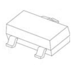
SOT-23 Plastic-Encapsulate MOSFETS
P-Channel Enhancement Mode Field Effect Transistor
General Description
The BC3407 uses advanced trench technology to provide excellent
RDS(on) with low gate charge. This device is suitable for use as a load
switch or in PWM applications.
SOT-23
1. GATE
2. SOURCE
3. DRAIN
MARKING: 3407
Maximum ratings (Ta=25℃ unless otherwise noted)
Parameter
Symbol
Drain-Source Voltage
VDS
Gate-Source Voltage
Value
-30
Unit
V
VGS
±20
V
Continuous Drain Current
ID
-4.1
A
Power Dissipation
PD
350
mW
RθJA
357
℃/W
Junction Temperature
TJ
150
℃
Storage Temperature
Tstg
-55~+150
℃
Thermal Resistance from Junction to Ambient
1 of 4
Copyright © All right reserved: Heyuan China Base Electronics Technology Co., Ltd.
�Electrical characteristics (Ta=25℃ unless otherwise noted)
Parameter
Symbol
Test Condition
Min
Typ
Max
Units
Static characteristics
Drain-source breakdown voltage
BVDSS
VGS = 0V, ID =-250µA
Zero gate voltage drain current
IDSS
VDS =-24V,VGS = 0V
-1
µA
Gate-source leakage current
IGSS
VGS =±20V, VDS = 0V
±100
nA
VGS =-10V, ID =-4.1A
60
mΩ
VGS =-4.5V, ID =-3A
87
mΩ
Drain-source on-resistance (note 1)
Forward tranconductance (note 1)
Gate threshold voltage
Diode forward voltage (note 1)
RDS(on)
gFS
VGS(th)
VSD
-30
VDS =-5V, ID =-4A
5.5
VDS =VGS, ID =-250µA
-1
V
S
IS=-1A,VGS=0V
-3
V
-1
V
Dynamic characteristics (note 2)
Input capacitance
Ciss
Output capacitance
Coss
Reverse transfer capacitance
700
pF
120
pF
Crss
75
pF
td(on)
8.6
ns
VGS=-10V,VDS=-15V,
5.0
ns
RL=3.6Ω,RGEN=3Ω
28.2
ns
13.5
ns
VDS =-15V,VGS =0V,f =1MHz
Switching Characteristics (note 2)
Turn-on delay time
Turn-on rise time
Turn-off delay time
Turn-off fall time
tr
td(off)
tf
Notes:
1.
2.
Pulse test: Pulse width ≤300µs, duty cycle ≤2%.
These parameters have no way to verify.
2 of 4
Copyright © All right reserved: Heyuan China Base Electronics Technology Co., Ltd.
�BC3407
Typical Characteristics
Output Characteristics
Transfer Characteristics
-25
-5
VGS=-10V
Ta=25℃
VGS=-4.5V
-8V
-5V
-20
-4
VGS=-3.5V
-10
ID
-15
-3
DRAIN CURRENT
DRAIN CURRENT
ID
(A)
(A)
VGS=-4V
-2
-5
-1
-0
-0
-0
-1
-2
-3
-4
DRAIN TO SOURCE VOLTAGE
RDS(ON)
VDS
-5
-0
(V)
-1
-2
GATE TO SOURCE VOLTAGE
-3
VGS
-4
(V)
RDS(ON) —— VGS
—— ID
140
100
Ta=25℃
Ta=25℃
120
(mΩ)
(mΩ)
80
100
RDS(ON)
60
ON-RESISTANCE
ON-RESISTANCE
RDS(ON)
VGS=-4.5V
VGS=-10V
40
80
ID=-4.3A
60
40
20
20
-2
-0
-4
-6
DRAIN CURRENT
IS
——
ID
-8
-10
-2
(A)
-4
-6
GATE TO SOURCE VOLTAGE
-8
VGS
(V)
VSD
-10
Ta=25℃
-0.1
SOURCE CURRENT
IS
(A)
-1
-0.01
-1E-3
-1E-4
-1E-5
-0.2
-0.4
-0.6
-0.8
SOURCE TO DRAIN VOLTAGE
-1.0
VSD
-1.2
(V)
3 of 4
Copyright © All right reserved: Heyuan China Base Electronics Technology Co., Ltd.
-10
�PACKAGE OUTLINE
Plastic surface mounted package; 3 leads
SOT-23
4 of 4
Copyright © All right reserved: Heyuan China Base Electronics Technology Co., Ltd.
�
很抱歉,暂时无法提供与“BC2301(2.8A) 复制”相匹配的价格&库存,您可以联系我们找货
免费人工找货