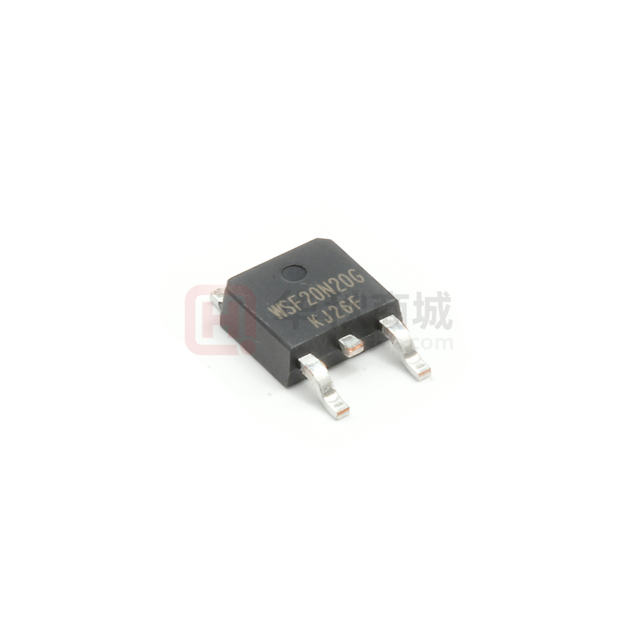
WSF20N20G
N-Ch MOSFET
General Description
Product Summery
The WSF20N20G is N-channel Enhanced
VDMOSFETs, is obtained by the self-aligned planar
Technology which reduce the conduction loss,
improve switching .
BVDSS
RDSON
ID
200V
0.12Ω
18A
Applications
performance and enhance the avalanche energy.
The transistor can be used in various power
switching circuit for system miniaturization and
higher efficiency..
z Uninterruptible Power Supply(UPS)
z Power Factor Correction (PFC)
Features
TO-252 Pin Configuration
z Advanced high cell density Trench technology
z Super Low Gate Charge
z Excellent Cdv/dt effect decline
z Green Device Available
Absolute Maximum Ratings
Symbol
Parameter
Rating
Units
VDS
Drain-Source Voltage
200
V
VGS
Gate-Source Voltage
ID@TC=25℃
ID@TC=100℃
IDM
±20
V
1
18
A
1
10
A
72
A
Continuous Drain Current, VGS @ 10V
Continuous Drain Current, VGS @ 10V
Pulsed Drain Current
2
EAS
Single Pulse Avalanche Energy
340
mJ
IAS
Avalanche Current
15
A
3
3
PD@TC=25℃
Total Power Dissipation
104
W
TSTG
Storage Temperature Range
-55 to 150
℃
TJ
Operating Junction Temperature Range
-55 to 150
℃
Thermal Data
Symbol
Parameter
Typ.
RθJA
Thermal Resistance Junction-ambient
RθJC
1
www.winsok.tw
Thermal Resistance Junction-Case
Page 1
1
Max.
Unit
---
60
℃/W
---
1.2
℃/W
Rev 1.0 Jun.2021
�WSF20N20G
N-Ch MOSFET
Electrical Characteristics (TJ=25 ℃, unless otherwise noted)
Symbol
BVDSS
Parameter
Conditions
Drain-Source Breakdown Voltage
VGS(th)
Max.
Unit
200
---
---
V
---
0.25
---
---
0.12
0.16
V/℃
Ω
2.0
3.5
4.0
V
---
-4.63
---
mV/℃
VDS=200V , VGS=0V , TJ=25℃
---
---
1
VDS=160V , VGS=0V , TJ=125℃
---
---
10
Reference to 25℃ , ID=1mA
2
Static Drain-Source On-Resistance
Gate Threshold Voltage
Typ.
VGS=0V , ID=250uA
△BVDSS/△TJ BVDSS Temperature Coefficient
RDS(ON)
Min.
VGS=10V , ID=4.5A
VGS=VDS , ID =250uA
△VGS(th)
VGS(th) Temperature Coefficient
IDSS
Drain-Source Leakage Current
IGSS
Gate-Source Leakage Current
VGS=±30V , VDS=0V
---
---
±100
nA
Rg
Gate Resistance
VDS=0V , VGS=0V , f=1MHz
---
0.12
---
Ω
Qg
Total Gate Charge (10V)
---
40
---
Qgs
Gate-Source Charge
---
5.2
---
---
18
---
---
24
---
---
45
---
---
101
---
Fall Time
---
95
---
Ciss
Input Capacitance
---
1317
---
Coss
Output Capacitance
---
181
---
Crss
Reverse Transfer Capacitance
---
76
---
Min.
Typ.
Max.
Unit
---
---
mJ
Min.
Typ.
Max.
Unit
---
---
18
A
---
---
72
A
---
---
1.4
V
---
230
---
nS
---
1.8
---
uC
Qgd
Td(on)
Tr
Td(off)
Tf
VDS=160V , VGS=10V , ID=18A
Gate-Drain Charge
Turn-On Delay Time
VDD=100V , VGS=10V ,
Rise Time
RG=25Ω,ID=18A
Turn-Off Delay Time
VDS=25V , VGS=0V , f=1MHz
uA
nC
ns
pF
Guaranteed Avalanche Characteristics
Symbol
EAS
Parameter
Conditions
5
Single Pulse Avalanche Energy
VDD=25V , L=0.1mH , IAS=15A
250
Diode Characteristics
Symbol
IS
ISM
Parameter
Continuous Source Current
2,6
Pulsed Source Current
2
VSD
Diode Forward Voltage
trr
Reverse Recovery Time
Qrr
Conditions
1,6
Reverse Recovery Charge
VG=VD=0V , Force Current
VGS=0V , IS=18A , TJ=25℃
IF=15A , dI/dt=100A/µs , TJ=25℃
Note :
1.The data tested by surface mounted on a 1 inch2 FR-4 board with 2OZ copper,t
很抱歉,暂时无法提供与“WSF20N20G”相匹配的价格&库存,您可以联系我们找货
免费人工找货- 国内价格
- 1+4.07550
- 10+3.12550
- 30+2.66000
- 100+2.18500
- 国内价格
- 1+3.47180
- 10+3.20480
- 30+2.93770
- 100+2.67060
- 国内价格
- 1+4.63320
- 10+3.55320
- 30+3.02400
- 100+2.48400