BF
BF356
Series
www.bfsemi.com
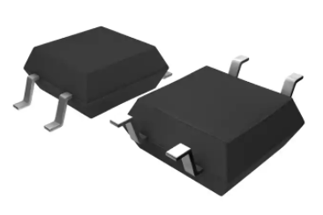
SOP4, DC Input Photo Transistor Coupler
SCHEMATIC
Description
The BF356 series combine an AlGaAs infrared
inf
emitting diode as the emitter which is optically
1
4
2
3
coupled to a silicon planar phototransistor
detector in a plastic SOP4 package.
package
With the robust coplanar double mold structure,
BF356 series provide the most stable isolation
feature.
Features
�
High isolation 3750 VRMS
�
CTR flexibility available see order
�
�
�
�
�
�
information
DC input with transistor output
Operating temperature range - 55 °C to
110 °C
PIN DEFINITION
1. Anode
2. Cathode
3. Emitter
4. Collector
PACKAGE OUTLINE
REACH compliance
Halogen free
MSL class 1
Regulatory Approvals
�
UL - UL1577
�
VDE - EN60747-5-5(VDE0884
5(VDE0884-5)
�
CQC – GB4943.1, GB8898
Applications
Switch mode power supplies
•
•
Programmable controllers
•
•
Household appliances
Office equipment
Document No: DWI-009
Rev:A00
Release Date: 2019/
9/8/12
1
�BF356 Series
www.bfsemi.com
SOP4, DC Input Photo Transistor Coupler
ABSOLUTE MAXIMUM RATINGS
PARAMETER
SYMBOL
VALUE
UNIT
NOTE
INPUT
Forward Current
IF
60
mA
Peak Forward Current
IFP
1
A
Reverse Voltage
VR
6
V
Input Power Dissipation
PI
100
mW
Collector - Emitter Voltage
VCEO
80
V
Emitter - Collector Voltage
VECO
7
V
Collector Current
IC
50
mA
Output Power Dissipation
PO
150
mW
Total Power Dissipation
Ptot
200
mW
Isolation Voltage
Viso
3750
Vrms
Operating Temperature
Topr
-55~110
°C
Storage Temperature
Tstg
-55~125
°C
Soldering Temperature
Tsol
260
°C
1
OUTPUT
COMMON
2
Note 1.100μs pulse, 100Hz frequency
Note 2. AC For 1 Minute, R.H. = 40 ~ 60%
Document No: DWI-009
Rev:A00
Release Date: 2019/8/12
2
�BF356 Series
www.bfsemi.com
SOP4, DC Input Photo Transistor Coupler
ELECTRICAL OPTICAL CHARACTERISTICS at Ta=25°C
PARAMETER
SYMBOL
MIN
TYP. MAX. UNIT
TEST CONDITION
NOTE
INPUT
Forward Voltage
VF
-
1.24
1.4
V
IF=10mA
Reverse Current
IR
-
-
10
µA
VR=6V
Input Capacitance
Cin
-
10
-
pF
V=0, f=1kHz
OUTPUT
Collector Dark Current
Collector-Emitter
Breakdown Voltage
Emitter-Collector
Breakdown Voltage
ICEO
-
-
100
nA
VCE=20V, IF=0
BVCEO
80
-
-
V
IC=0.1mA, IF=0
BVECO
7
-
-
V
IE=0.1mA, IF=0
TRANSFER CHARACTERISTICS
BF356
50
-
600
Current
BF356A
80
-
160
Transfer
Ratio
BF356B
130
-
260
BF356C
200
-
400
BF356D
300
-
600
-
0.06
Collector-Emitter
Saturation Voltage
CTR
VCE(sat)
10^12 10^14
%
IF=5mA, VCE=5V
0.2
V
IF=20mA, IC=1mA
-
Ω
DC500V, 40 ~ 60% R.H.
Isolation Resistance
RISO
Floating Capacitance
CIO
-
0.4
1
pF
V=0, f=1MHz
Cut-off Frequency
fc
-
80
-
kHz
VCE=2V, IC=2mA
RL=100Ω,-3dB
Response Time (Rise)
tr
-
3
18
µs
Response Time (Fall)
tf
-
4
18
µs
VCE=2V, IC=2mA
RL=100Ω
4
3
3
Note 3. Fig.12&13
Note 4. Fig.14
Document No: DWI-009
Rev:A00
Release Date: 2019/8/12
3
�BF
BF356
Series
www.bfsemi.com
SOP4, DC Input Photo Transistor Coupler
CHARACTERISTIC CURVES
Fig.1 Forward Current
vs. Ambient Temperature
Fig.2 Collector Power Dissipation
vs.Ambient Temperature
Fig.3 Forward Current
vs. Forward Voltage
Fig.4 Collector Dark Current
vs.Ambient Temperature
Fig.5 Collector Current
Fig.6 Collector Current
vs. Collector-emitter
emitter Voltage
vs. Collector-emitter
emitter Voltage
Document No: DWI-009
Rev:A00
Release Date: 2019/
9/8/12
4
�BF
BF356
Series
www.bfsemi.com
SOP4, DC Input Photo Transistor Coupler
CHARACTERISTICCURVES
Fig.7 Normalized Current Transfer Ratio
vs. Forward Current
Fig.8 Normalized Current Transfer Ratio
vs.Ambient Temperature
Fig.9 Collector-emitter
emitter Saturation Voltage
vs. Ambient Temperature
Fig.10 Switching Time
vs.Load Resistance
Fig.11 Frequency Response
Document No: DWI-009
Rev:A00
Release Date: 2019/
9/8/12
5
�BF
BF356
Series
www.bfsemi.com
SOP4, DC Input Photo Transistor Coupler
TEST CIRCUITS
Fig.12 Test Circuits of Response Time
Fig.13Curves
s of Response Time
Fig.14Test Circuits of Frequency Response
Document No: DWI-009
Rev:A00
Release Date: 2019/
9/8/12
6
�BF
BF356
Series
www.bfsemi.com
SOP4, DC Input Photo Transistor Coupler
PACKAGE DIMENSIONS (Dimensions in mm unless otherwise stated)
Recommended Solder Mask (Dimensions in mm unless otherwise stated)
Document No: DWI-009
Rev:A00
Release Date: 2019/
9/8/12
7
�BF
BF356
Series
www.bfsemi.com
SOP4, DC Input Photo Transistor Coupler
CARRIER
ARRIER TAPE SPECIFICATIONS (Dimensions in mm unless otherwise stated)
Option T1
Option T2
Document No: DWI-009
Rev:A00
Release Date: 2019/
9/8/12
8
�BF
BF356
Series
www.bfsemi.com
SOP4, DC Input Photo Transistor Coupler
REEL SPECIFICATIONS (Dimensions in mm unless otherwise stated)
Option T1 & T2
Document No: DWI-009
Rev:A00
Release Date: 2019/
9/8/12
9
�BF356 Series
www.bfsemi.com
SOP4, DC Input Photo Transistor Coupler
BOX SPECIFICATIONS (Reel Type)
Inner Box
�
L x W x H = 36cm x 36cm x 6.9cm
Outer Box
�
L x W x H = 45cm x 38cm x 38cm
Document No: DWI-009
Rev:A00
Release Date: 2019/8/12
10
�BF356 Series
www.bfsemi.com
SOP4, DC Input Photo Transistor Coupler
ORDERING AND MARKING INFORMATION
MARKING INFORMATION
BF
356
X
V
Y
A
WW
BF
356X
VYAWW
: Company Abbr.
: Part Number
: CTR Rank
: VDE Option
: Fiscal Year
: Manufacturing Code
: Work Week
ORDERING INFORMATION
LABEL INFORMATION
BF356X(Z)-GV
BF – Company Abbr.
356 – Part Number
X – Rank (A/B/C/D or None)
Z – Tape and Reel Option (T1/T2)
G – Green
V – VDE Option (V or None)
PACKING QUANTITY
Option
Quantity
Quantity – Inner box
Quantity – Outer box
T1
3000 Units/Reel
3 Reels/Inner box
5 Inner box/Outer box = 45k Units
T2
3000 Units/Reel
3 Reels/Inner box
5 Inner box/Outer box = 45k Units
Document No: DWI-009
Rev:A00
Release Date: 2019/8/12
11
�BF356 Series
www.bfsemi.com
SOP4, DC Input Photo Transistor Coupler
REFLOW INFORMATION
REFLOW PROFILE
Profile Feature
Sn-Pb Assembly Profile
Pb-Free Assembly Profile
Temperature Min. (Tsmin)
100
150°C
Temperature Max. (Tsmax)
150
200°C
Time (ts) from (Tsmin to Tsmax)
60-120 seconds
60-120 seconds
Ramp-up Rate (tL to tP)
3°C/second max.
3°C/second max.
Liquidous Temperature (TL)
183°C
217°C
Time (tL) Maintained Above (TL)
60 – 150 seconds
60 – 150 seconds
Peak Body Package Temperature
235°C +0°C / -5°C
260°C +0°C / -5°C
Time (tP) within 5°C of 260°C
20 seconds
30 seconds
Ramp-down Rate (TP to TL)
6°C/second max
6°C/second max
Time 25°C to Peak Temperature
6 minutes max.
8 minutes max.
Document No: DWI-009
Rev:A00
Release Date: 2019/8/12
12
�BF356 Series
www.bfsemi.com
SOP4, DC Input Photo Transistor Coupler
DISCLAIMER
�
BF SEMICONDUCTOR is continually improving the quality, reliability, function and design. BF
SEMICONDUCTOR reserves the right to make changes without further notices.
�
The characteristic curves shown in this datasheet are representing typical performance which are
not guaranteed.
�
BF SEMICONDUCTOR makes no warranty, representation or guarantee regarding the suitability of
the products for any particular purpose or the continuing production of any product. To the
maximum extent permitted by applicable law, BF SEMICONDUCTOR disclaims (a) any and all
liability arising out of the application or use of any product, (b) any and all liability, including without
limitation special, consequential or incidental damages, and (c) any and all implied warranties,
including warranties of fitness for particular
�
The products shown in this publication are designed for the general use in electronic applications
such as office automation, equipment, communications devices, audio/visual equipment, electrical
application and instrumentation purpose, non-infringement and merchantability.
�
This product is not intended to be used for military, aircraft, automotive, medical, life sustaining or
lifesaving applications or any other application which can result in human injury or death.
�
Please contact BF SEMICONDUCTOR sales agent for special application request.
�
Immerge unit’s body in solder paste is not recommended.
�
Parameters provided in datasheets may vary in different applications and performance may vary
over time. All operating parameters, including typical parameters, must be validated in each
customer application by the customer’s technical experts. Product specifications do not expand or
otherwise modify BF SEMICONDUCTOR’s terms and conditions of purchase, including but not
limited to the warranty expressed therein.
�
Discoloration might be occurred on the package surface after soldering, reflow or long-time use. It
neither impacts the performance nor reliability.
Document No: DWI-009
Rev:A00
Release Date: 2019/8/12
13
�