LNC5N50\LND5N50\LNG5N50\LNH5N50
Lonten N-channel 500V, 5A Power MOSFET
Description
Product Summary
The Power MOSFET is fabricated using the
VDSS
500V
advanced
ID
5A
planar
VDMOS
technology.
The
resulting device has low conduction resistance,
RDS(on),max
1.6Ω
superior switching performance and high avalanche
Qg,typ
12.8 nC
energy.
Features
Low RDS(on)
Low gate charge (typ. Qg = 12.8 nC)
100% UIS tested
RoHS compliant
TO-251
TO-252
TO-220
TO-220F
D
Applications
G
Power factor correction.
Switched mode power supplies.
LED driver.
S
N-Channel MOSFET
Pb
Absolute Maximum Ratings
Parameter
Symbol
Drain-Source Voltage
VDSS
Continuous drain current
( TC = 25°C )
ID
Avalanche energy, single pulse
Peak diode recovery dv/dt
2)
V
A
A
20
A
VGSS
±30
V
EAS
210
mJ
5
V/ns
30
W
0.24
W/°C
75
W
0.6
W/°C
-55 to +150
°C
dv/dt
3)
500
5
IDM
Gate-Source voltage
Unit
3.1
( TC = 100°C )
Pulsed drain current 1)
Value
Power Dissipation TO-220F ( TC = 25°C )
Derate above 25°C
PD
Power Dissipation
TO-220\TO-251\TO-252 ( TC = 25°C )
Derate above 25°C
Operating junction and storage temperature range
TJ, TSTG
Continuous diode forward current
IS
5
A
Diode pulse current
IS,pulse
20
A
Thermal Characteristics
Parameter
Symbol
Value
TO-220F
TO-220\TO-251\TO-252
Unit
Thermal resistance, Junction-to-case
RθJC
4.17
1.67
°C/W
Thermal resistance, Junction-to-ambient
RθJA
62.5
110
°C/W
Version 1.2,Jan-2020
1
www.lonten.cc
�LNC5N50\LND5N50\LNG5N50\LNH5N50
Package Marking and Ordering Information
Device
Device Package
Marking
Units/Tube
LNC5N50
TO-220
LNC5N50
50
LND5N50
TO-220F
LND5N50
50
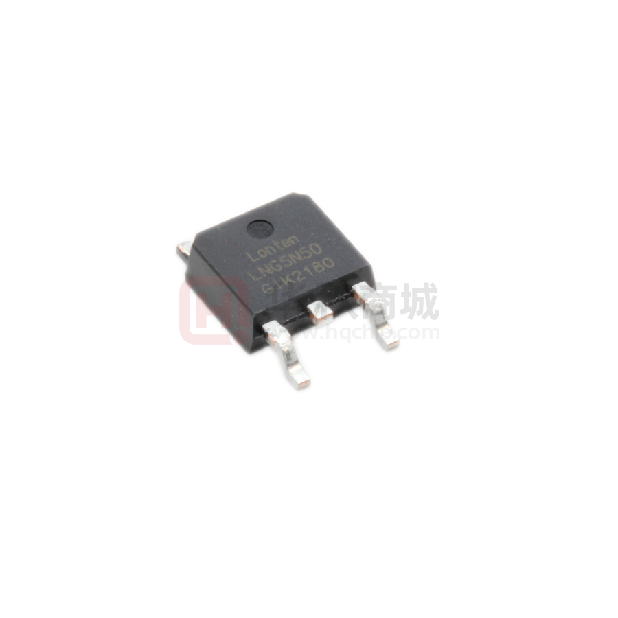
LNG5N50
TO-252
LNG5N50
LNH5N50
TO-251
LNH5N50
Electrical Characteristics
Parameter
Units/Reel
3000
80
Tc = 25°C unless otherwise noted
Symbol
Test Condition
Min.
Typ.
Max.
Unit
Static characteristics
Drain-source breakdown voltage
BVDSS
VGS=0 V, ID=0.25 mA
500
-
-
V
Gate threshold voltage
VGS(th)
VDS=VGS, ID=0.25 mA
2
-
4
V
Drain cut-off current
IDSS
VDS=500 V, VGS=0 V,
Tj = 25°C
-
-
1
μA
Tj = 125°C
-
100
Gate leakage current, Forward
IGSSF
VGS=30 V, VDS=0 V
-
-
100
nA
Gate leakage current, Reverse
IGSSR
VGS=-30 V, VDS=0 V
-
-
-100
nA
Drain-source on-state resistance
RDS(on)
VGS=10 V, ID=2.5 A
-
1.35
1.60
Ω
Input capacitance
Ciss
VDS = 25 V, VGS = 0 V,
-
537.5
-
Output capacitance
Coss
f = 1 MHz
-
80.3
-
Reverse transfer capacitance
Crss
-
4
-
Turn-on delay time
td(on)
VDD = 250 V, ID = 5 A
-
10.3
-
Rise time
tr
RG = 10 Ω, VGS=15 V
-
33.1
-
Turn-off delay time
td(off)
-
29.4
-
Fall time
tf
-
13.2
Dynamic characteristics
pF
ns
-
Gate charge characteristics
Gate to source charge
Qgs
VDD=400 V, ID=5 A,
-
3.9
-
Gate to drain charge
Qgd
VGS=0 to 10 V
-
4.6
-
Gate charge total
Qg
-
12.8
-
Gate plateau voltage
Vplateau
-
5
-
V
nC
Reverse diode characteristics
Diode forward voltage
VSD
VGS=0 V, IF=5 A
-
-
1.5
V
Reverse recovery time
trr
VR=250 V, IF=5 A,
-
319.2
-
ns
Reverse recovery charge
Qrr
dIF/dt=100 A/μs
-
1.6
-
μC
Peak reverse recovery current
Irrm
-
10.2
-
A
Notes:
1. Pulse width limited by maximum junction temperature.
2. L=10mH, IAS = 6.5A, Starting Tj= 25°C.
3. ISD = 5A, di/dt≤100A/us, VDD≤BVDS, Starting Tj= 25°C.
Version 1.2,Jan-2020
2
www.lonten.cc
�LNC5N50\LND5N50\LNG5N50\LNH5N50
Electrical Characteristics Diagrams
Figure 1. Typical Output Characteristics
Figure 2. Transfer Characteristics
VGS=10V
VGS=9V
VGS=6V
VGS=8V
Tc = 25°C
VGS=7V
VGS=5.5V
Tc = 150°C
VDS ,Drain−source voltage (V)
VGS ,Gate−source voltage (V)
Figure 3. On-Resistance Variation vs. Drain Current
Figure 4. Threshold Voltage vs. Temperature
VGS = 10 V
Tc = 25°C
Pulse test
IDS=0.25 mA
Pulse test
ID ,Drain current (A)
Tj ,Junction temperature (°C)
Figure 5. Breakdown Voltage vs. Temperature
Figure 6. On-Resistance vs. Temperature
VGS=10 V
IDS=2.5 A
Pulse test
VGS=0 V
IDS=0.25 mA
Pulse test
Tj ,Junction temperature (°C)
Tj ,Junction temperature (°C)
Version 1.2,Jan-2020
3
www.lonten.cc
�LNC5N50\LND5N50\LNG5N50\LNH5N50
Figure 7. Capacitance Characteristics
Figure 8. Gate Charge Characteristics
VDS=250
Ciss
Notes:f = 1 MHz,VGS=0 V
Ciss = Cgs + Cgd (Cds = shorted)
Coss = Cds + Cgd
Crss = Cgd
Coss
Crss
ID = 5 A
VDS ,Drain-Source Voltage (V)
QG ,Total Gate Charge (nC)
Figure 9. Maximum Safe Operating Area
Figure 10. Maximum Safe Operating Area
TO-220F
TO-220/TO-251/TO-252
100us
100us
10ms
Limited by RDS(on)
1ms
10ms
1ms
Limited by RDS(on)
DC
Notes:
T = 25°C
c
Notes:
T = 25°C
j
T = 150°C
c
T = 150°C
j
Single Pulse
Single Pulse
VDS ,Drain-Source Voltage (V)
VDS ,Drain-Source Voltage (V)
Figure 11. Power Dissipation vs. Temperature
Figure 12. Power Dissipation vs. Temperature
TO-220F
TO-220/TO-251/TO-252
Tc ,Case temperature (°C)
Version 1.2,Jan-2020
DC
Tc ,Case temperature (°C)
4
www.lonten.cc
�LNC5N50\LND5N50\LNG5N50\LNH5N50
Figure 13. Continuous Drain Current vs. Temperature
Figure 14. Body Diode Transfer Characteristics
Tc = 150°
C
Tc = 25°C
VSD ,Source-Drain Voltage (V)
Tc ,Case temperature (°C)
Figure 15 Transient Thermal Impedance, Junction to Case, TO-220F
P
DM
In descending order
D= 0.5, 0.2, 0.1, 0.05, 0.02, 0.01, single pulse
t
Duty = t/T
T
Z (t)=4.17°C/W Max.
θJC
t ,Pulse Width (s)
Figure 16. Transient Thermal Impedance, Junction to Case, TO-220/TO-251/TO-252
In descending order
D= 0.5, 0.2, 0.1, 0.05, 0.02, 0.01, single pulse
P
DM
t
Duty = t/T
Z (t)=1.67°C/W Max.T
θJC
t ,Pulse Width (s)
Version 1.2,Jan-2020
5
www.lonten.cc
�LNC5N50\LND5N50\LNG5N50\LNH5N50
Gate Charge Test Circuit & Waveform
Switching Test Circuit & Waveforms
Unclamped Inductive Switching Test Circuit & Waveforms
Version 1.2,Jan-2020
6
www.lonten.cc
�LNC5N50\LND5N50\LNG5N50\LNH5N50
Mechanical Dimensions for TO-220
UNIT:mm
SYMBOL
MIN
NOM
A
4
4.8
B
1.2
1.4
B1
1
1.4
b1
0.75
0.95
c
0.4
0.55
D
15
16.5
D1
5.9
6.9
E
9.9
10.7
e
2.44
F
1.1
1.4
L
12.5
14.5
L1
3
3.5
4
ΦP
3.7
3.8
3.9
Q
2.5
3
Q1
2
2.9
Y
8.02
2.54
8.12
MAX
2.64
8.22
TO-220 Part Marking Information
Lonten Logo
“AB”
Foundry & Assembly Code
Lonten
G LNC5N50
ABYWW99
Part Number
“99”
Manufacturing Code
“YWW”
Date Code
Version 1.2,Jan-2020
7
www.lonten.cc
�LNC5N50\LND5N50\LNG5N50\LNH5N50
Mechanical Dimensions for TO-220F
UNIT:mm
SYMBOL
MIN
NOM
MAX
A
4.5
4.9
A1
2.3
2.9
b
0.65
0.9
b1
1.1
1.7
b2
1.2
1.4
c
0.35
0.65
D
14.5
16.5
D1
6.1
6.9
E
9.6
10.3
E1
6.5
7
7.5
e
2.44
2.54
2.64
L
12.5
14.3
L1
9.45
10.05
L2
15
16
L3
3.2
4.4
ΦP
3
3.3
Q
2.5
2.9
TO-220F Part Marking Information
Lonten Logo
“AB”
Foundry & Assembly Code
“YWW”
Date Code
Version 1.2,Jan-2020
Lonten
LND5N50
ABYWW99
Part Number
“99”
Manufacturing Code
8
www.lonten.cc
�LNC5N50\LND5N50\LNG5N50\LNH5N50
Mechanical Dimensions for TO-252
UNIT:mm
SYMBOL
MIN
NOM
A
2.10
2.50
B
0.80
1.25
b
0.50
0.85
b1
0.50
0.90
b2
0.45
0.60
C
0.45
0.60
D
6.35
6.75
D1
5.10
5.50
E
5.80
6.30
e1
2.25
e2
4.45
4.75
L1
9.50
10.20
L2
0.90
1.45
L3
0.60
1.10
K
-0.1
0.10
2.30
MAX
2.35
TO-252 Part Marking Information
Lonten Logo
“AB”
Foundry & Assembly Code
Lonten
LNG5N50
ABYWW99
Part Number
“99”
Manufacturing Code
“YWW”
Date Code
Version 1.2,Jan-2020
9
www.lonten.cc
�LNC5N50\LND5N50\LNG5N50\LNH5N50
Mechanical Dimensions for TO-251
UNIT:mm
SYMBOL
MIN
A
2.10
2.50
A1
0.95
1.30
B
0.80
1.25
b
0.50
0.80
b1
0.70
0.90
C
0.45
0.60
C1
0.45
0.60
D
6.35
6.75
D1
5.10
5.50
E
5.80
6.30
e
2.25
L
7.70
8.50
L1
1.45
1.95
R
NOM
2.30
MAX
2.35
0.30
TO-251 Part Marking Information
Lonten Logo
“AB”
Foundry & Assembly Code
Lonten
LNH5N50
ABYWW99
Part Number
“99”
Manufacturing Code
“YWW”
Date Code
Version 1.2,Jan-2020
10
www.lonten.cc
�LNC5N50\LND5N50\LNG5N50\LNH5N50
Disclaimer
The content specified herein is for the purpose of introducing LONTEN's products (hereinafter "Products"). The
information given in this document shall in no event be regarded as a guarantee of conditions or characteristics.
Examples of application circuits, circuit constants and any other information contained herein illustrate the
standard usage and operations of the Products. The peripheral conditions must be taken into account when
designing circuits for mass production.
LONTEN does not assume any liability for infringement of patents, copyrights, or other intellectual property rights
of third parties by or arising from the use of the Products or technical information described in this document.
The Products are not designed or manufactured to be used with any equipment, device or system which requires
an extremely high level of reliability the failure or malfunction of which may result in a direct threat to human life or
create a risk of human injury (such as a medical instrument, transportation equipment, aerospace machinery,
nuclear-reactor controller, fuel-controller or other safety device). LONTEN shall bear no responsibility in any way
for use of any of the Products for the above special purposes.
Although LONTEN endeavors to improve the quality and reliability of its products, semiconductor products have
specific characteristics such as the occurrence of failure at a certain rate and malfunctions under certain use
conditions. Please be sure to implement safety measures to guard them against the possibility of physical injury,
and injury or damage caused by fire in the event of the failure of a LONTEN product.
The content specified herein is subject to change for improvement without notice. When using a LONTEN product,
be sure to obtain the latest specifications.
Version 1.2,Jan-2020
11
www.lonten.cc
�