LTC8631, LTC8632, LTC8634
P-1
General Description
The LTC863x family of single-, dual-, and quad- channel operational amplifiers
represents a new generation of general-purpose, low-power op-amps. Featuring railto-rail input and output (RRIO) swings, low quiescent current (typical 700 µA) combined
with a wide bandwidth (9 MHz) and very low noise (13 nV/√Hz at 1 kHz) makes this family
very attractive for a variety of battery-powered applications that require a good balance
between cost and performance, such as audio outputs, motor phase current sensing,
photodiode amplification, barcode scanners and white goods. The low input bias current
supports these amplifiers to be used in applications with mega-ohm source impedances.
The robust design of the LTC863x amplifiers provides ease-of-use to the circuit designer:
unity-gain stability with capacitive loads of up to 500 pF, integrated RF/EMI rejection
filter, no phase reversal in overdrive conditions, and high electro-static discharge (ESD)
protection (5-kV HBM). The LTC863x amplifiers are optimized for operation at voltages
as low as +2.3 V (±1.15 V) and up to +5.5 V (±2.75 V) over the extended temperature
range of −40 ℃ to +125 ℃.
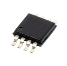
The LTC8631 (single) is available in SOT23-5L package. The LTC8632 (dual) is offered in
both SOIC-8L, DFN-8L and MSOP8L packages. The quad-channel LTC8634 is offered in
14- lead SOIC package.
Features and Benefits
Wide Unity-Gain Bandwidth: 9 MHz
High Slew Rate: 8.5 V/μs
Fast Settling: 0.3 μs to 0.1%
Low Noise: 13 nV/√Hz at 1 kHz
Low Input Offset Voltage: ±0.7 mV
Single 2.3 V to 5.5 V Power Supply Range
Rail-to-Rail Input and Output
Internal RF/EMI Filter
Low Supply Current: 700 μA at 5V Supply Per Amplifier
Extended Temperature Range: −40℃ to +125℃
Motor Phase Current Sense
Photodiode Amplification
Audio Outputs
Active Filters
Driving A/D Converters
Portable Equipment
Battery-Powered Instrumentation
Applications
Pin Configurations (Top View)
OUT
1
–VS
2
+IN
3
LTC8631
LTC8632
LTC8632
LTC8634
SOT23-5L
DFN2x2-8L
SOIC-8L / MSOP-8L
SOIC-14L
5
4
+VS
–IN
OUTA 1
8
+VS
–INA 2
7
OUTB
+INA 3
6
–INB
–VS 4
5
+INB
OUTA
1
–INA
2
A
14
OUTD
13
–IND
12
+IND
4
11
–VS
5
10
+INC
OUTA
1
OUTB
–INA
2
6
–INB
+INA
3
5
+INB
+VS
+INB
8
+VS
7
A
+INA
3
–VS
4
B
B
CAUTION: These devices are sensitive to electrostatic discharge; follow proper IC Handling Procedures.
Linearin and designs are registered trademarks of Linearin Technology Corporation.
© Copyright Linearin Technology Corporation. All Rights Reserved.
All other trademarks mentioned are the property of their respective owners.
D
C
–INB
6
9
–INC
OUTB
7
8
OUTC
FN1617-41L.1d — Data Sheet
9MHz, High Slew Rate, RRIO, CMOS Amplifiers
�LTC8631, LTC8632, LTC8634
P-2
Pin Description
Symbol
Description
–IN
Inverting input of the amplifier. The voltage range is from (VS– – 0.1V) to (VS+ + 0.1V).
+IN
Non-inverting input of the amplifier. This pin has the same voltage range as –IN.
+VS
Positive power supply. The voltage is from 2.3V to 5.5V. Split supplies are possible
as long as the voltage between VS+ and VS– is from 2.3V to 5.5V.
–VS
Negative power supply. It is normally tied to ground. It can also be tied to a voltage
other than ground as long as the voltage between VS+ and VS– is from 2.3V to 5.5V.
OUT
Amplifier output.
Ordering Information
Type Number
Package Name
Package Quantity
Marking Code (1)
LTC8631XT5/R6
SOT23-5L
Tape and Reel, 3 000
AH1
LTC8632XS8/R8
SOIC-8L
Tape and Reel, 4 000
C32 /X
LTC8632XF8/R6
DFN2x2-8L
Tape and Reel, 3 000
AH2x, C32X
LTC8632XV8/R6
MSOP-8L
Tape and Reel, 3 000
AH2x, C32X
LTC8634XS14/R5
SOIC-14L
Tape and Reel, 2 500
C34 /X
(1) There may be multiple device markings, a varied marking character of “x” , or additional marking, which relates to the
logo, the lot trace code information, or the environmental category on the device.
Limiting Value
In accordance with the Absolute Maximum Rating System (IEC 60134).
Parameter
Absolute Maximum Rating
Supply Voltage, VS+ to VS–
10.0 V
Signal Input Terminals: Voltage, Current
VS– – 0.5 V to VS+ + 0.5 V, ±10 mA
Output Short-Circuit
Continuous
Storage Temperature Range, Tstg
–65 ℃ to +150 ℃
Junction Temperature, TJ
150 ℃
Lead Temperature Range (Soldering 10 sec)
260 ℃
ESD Rating
Parameter
Electrostatic
Discharge
Voltage
Item
Human body model (HBM), per MIL-STD-883J / Method 3015.9
Value
(1)
Unit
±5 000
Charged device model (CDM), per ESDA/JEDEC JS-002-2014 (2)
±2 000
Machine model (MM), per JESD22-A115C
±250
V
(1) JEDEC document JEP155 states that 500-V HBM allows safe manufacturing with a standard ESD control process.
Manufacturing with less than 500-V HBM is possible if necessary precautions are taken.
(2) JEDEC document JEP157 states that 250-V CDM allows safe manufacturing with a standard ESD control process.
Manufacturing with less than 250-V CDM is possible if necessary precautions are taken.
CAUTION: These devices are sensitive to electrostatic discharge; follow proper IC Handling Procedures.
Linearin and designs are registered trademarks of Linearin Technology Corporation.
© Copyright Linearin Technology Corporation. All Rights Reserved.
All other trademarks mentioned are the property of their respective owners.
FN1617-41L.1d — Data Sheet
9MHz, High Slew Rate, RRIO, CMOS Amplifiers
�LTC8631, LTC8632, LTC8634
P-3
Electrical Characteristics
VS = 5.0V, TA = +25℃, VCM = VS /2, VO = VS /2, and RL = 10kΩ connected to VS /2, unless otherwise noted.
Boldface limits apply over the specified temperature range, TA = −40 to +125 ℃.
Symbol
Parameter
Conditions
Min.
Typ.
Max.
±0.7
±3.5
Unit
OFFSET VOLTAGE
VOS
Input offset voltage
VOS TC
Offset voltage drift
TA = −40 to +125 ℃
Power supply
rejection ratio
VS = 2.3 to 5.5 V, VCM < VS+ − 2V
90
TA = −40 to +125 ℃
77
PSRR
mV
μV/℃
±2
106
dB
INPUT BIAS CURRENT
1
IB
IOS
Input bias current
TA = +85 ℃
150
TA = +125 ℃
500
Input offset current
pA
1
pA
f = 0.1 to 10 Hz
4.2
μVP-P
f = 1 kHz
13
nV/√Hz
f = 1 kHz
5
fA/√Hz
NOISE
Vn
en
In
Input voltage noise
Input voltage noise
density
Input current noise
density
INPUT VOLTAGE
VCM
CMRR
Common-mode
voltage range
Common-mode
rejection ratio
VS––0.1
VCM = −0.1 to 5.1 V
70
VCM = 0 to 4.9 V, TA = −40 to +125 ℃
67
VS = 2.3 V, VCM = −0.1 to 2.1 V
66
VCM = 0 to 2.1 V, TA = −40 to +125 ℃
62
VS++0.1
V
82
77
dB
INPUT IMPEDANCE
CIN
Input capacitance
Differential
2.0
Common mode
3.5
pF
OPEN-LOOP GAIN
AVOL
Open-loop voltage
gain
RL = 10 kΩ, VO = 0.05 to 3.5 V
93
TA = −40 to +125 ℃
84
RL = 600 Ω, VO = 0.15 to 3.5 V
78
TA = −40 to +125 ℃
70
102
87
dB
FREQUENCY RESPONSE
GBW
Gain bandwidth
product
SR
Slew rate
G = +1, CL = 100 pF, VO = 1.5 to 3.5 V
THD+N
Total harmonic
distortion + noise
G = +1, f = 1 kHz, VO = 0.5 VRMS
tS
Settling time
tOR
Overload recovery
time
9
MHz
8.5
V/μs
0.0008
%
To 0.1%, G = +1, 1V step
0.3
To 0.01%, G = +1, 1V step
0.4
VIN * Gain > VS
0.3
CAUTION: These devices are sensitive to electrostatic discharge; follow proper IC Handling Procedures.
Linearin and designs are registered trademarks of Linearin Technology Corporation.
© Copyright Linearin Technology Corporation. All Rights Reserved.
All other trademarks mentioned are the property of their respective owners.
μs
μs
FN1617-41L.1d — Data Sheet
9MHz, High Slew Rate, RRIO, CMOS Amplifiers
�LTC8631, LTC8632, LTC8634
P-4
Electrical Characteristics (continued)
VS = 5.0V, TA = +25℃, VCM = VS /2, VO = VS /2, and RL = 10kΩ connected to VS /2, unless otherwise noted.
Boldface limits apply over the specified temperature range, TA = −40 to +125 ℃.
Symbol
Parameter
Conditions
Min.
Typ.
Max.
Unit
OUTPUT
VOH
High output voltage
swing
RL = 10 kΩ
VS+–14
VS+–10
RL = 600 Ω
VS+–200
VS+–140
VOL
Low output voltage
swing
RL = 10 kΩ
VS–+7
VS–+10
RL = 600 Ω
VS–+100
VS–+150
ISC
Short-circuit current
mV
±70
mV
mA
POWER SUPPLY
VS
Operating supply
voltage
TA = −40 to +125 ℃
IQ
Quiescent current
(per amplifier)
VS = 2.5 V
600
730
VS = 5.0 V
700
850
2.3
5.5
V
μA
THERMAL CHARACTERISTICS
TA
θJA
Operating
temperature range
Package Thermal
Resistance
–40
+125
SOT23-5L
190
DFN2x2-8L
94
MSOP-8L
216
SOIC-8L
125
SOIC-14L
115
CAUTION: These devices are sensitive to electrostatic discharge; follow proper IC Handling Procedures.
Linearin and designs are registered trademarks of Linearin Technology Corporation.
© Copyright Linearin Technology Corporation. All Rights Reserved.
All other trademarks mentioned are the property of their respective owners.
℃
℃/W
FN1617-41L.1d — Data Sheet
9MHz, High Slew Rate, RRIO, CMOS Amplifiers
�LTC8631, LTC8632, LTC8634
P-5
Typical Performance Characteristics
100 mV/div
1 V/div
At TA = +25℃, VCM = VS /2, and RL = 10kΩ connected to VS /2, unless otherwise noted.
CL = 100pF
AV = +1
CL = 100pF
AV = +1
0.25 µs/div
100 ns/div
Small Signal Step Response (500 mV).
Voltage Noise (nV/√Hz)
Large Signal Step Response.
25 mV/div
100
CL = 100pF
AV = +1
10
1
1
Small Signal Step Response (500 mV).
10k
1M
Input Voltage Noise Spectral Density as a function of
Frequency.
120
125
100
100
80
PSRR (dB)
CMRR (dB)
100
Frequency (Hz)
100 ns/div
60
40
75
50
25
20
0
0
1
100
10k
1M
1
Frequency (Hz)
Common-mode Rejection Ratio as a function of
Frequency.
100
10k
1M
Frequency (Hz)
Power Supply Rejection Ratio as a function of
Frequency.
CAUTION: These devices are sensitive to electrostatic discharge; follow proper IC Handling Procedures.
Linearin and designs are registered trademarks of Linearin Technology Corporation.
© Copyright Linearin Technology Corporation. All Rights Reserved.
All other trademarks mentioned are the property of their respective owners.
FN1617-41L.1d — Data Sheet
9MHz, High Slew Rate, RRIO, CMOS Amplifiers
�LTC8631, LTC8632, LTC8634
P-6
Typical Performance Characteristics (continued)
At TA = +25℃, VCM = VS /2, and RL = 10kΩ connected to VS /2, unless otherwise noted.
120
160
5
90
120
4
60
80
30
40
0
0
Output Voltage (V)
Phase (deg)
AOL (dB)
Sourcing Current
–40℃
3
+125℃
2
+25℃
1
Sinking Current
-30
0
-40
10
1k
100k
0
10M
20
Frequency (Hz)
80
100
Output Voltage Swing as a function of Output
Current.
125
Short-circuit Current (mA)
100
Short-circuit Current (mA)
60
Output Current (mA)
Open-loop Gain and Phase as a function of
Frequency.
80
– ISC
60
40
+ISC
20
VS = 5V
100
75
50
25
0
0
1.5
2
2.5
3
3.5
4
4.5
5
-50
5.5
-25
0
25
50
75
100
125
Temperature (℃)
Supply Voltage (V)
Short-circuit Current as a function of Supply
Voltage.
Short-circuit Current as a function of Temperature.
1000
1,000
900
900
Quiescent Current (μA)
Quiescent Current (μA)
40
800
700
600
500
400
300
200
VS = 5V
800
700
600
500
400
300
200
100
100
0
0
2
2.5
3
3.5
4
4.5
5
5.5
-50
0
25
50
75
100
125
Temperature (℃)
Supply Voltage (V)
Quiescent Current as a function of Supply Voltage.
-25
Quiescent Current as a function of Temperature.
CAUTION: These devices are sensitive to electrostatic discharge; follow proper IC Handling Procedures.
Linearin and designs are registered trademarks of Linearin Technology Corporation.
© Copyright Linearin Technology Corporation. All Rights Reserved.
All other trademarks mentioned are the property of their respective owners.
FN1617-41L.1d — Data Sheet
9MHz, High Slew Rate, RRIO, CMOS Amplifiers
�P-7
LTC8631, LTC8632, LTC8634
Application Notes
The LTC863x is a family of low-power, rail-to-rail
input and output operational amplifiers specifically
designed for portable applications. These devices
operate from 2.3 V to 5.5 V at the temperature range
of –40 ℃ to +125 ℃, are unity-gain stable, and
suitable for a wide range of general-purpose
applications. The class AB output stage is capable of
driving ≤ 10-kΩ loads connected to any point
between VS+ and ground. The input common-mode
voltage range includes both rails, and allows the
LTC863x family to be used in virtually any singlesupply application. Rail-to-rail input and output
swing significantly increases dynamic range,
especially in low-supply applications, and makes
them ideal for driving sampling analog-to-digital
converters (ADCs).
The typical input bias current of the LTC863x during
normal operation is approximately 1-pA. In
overdriven conditions, the bias current can increase
significantly. The most common cause of an
overdriven condition occurs when the operational
amplifier is outside of the linear range of operation.
When the output of the operational amplifier is driven
to one of the supply rails, the feedback loop
requirements cannot be satisfied and a differential
input voltage develops across the input pins. This
differential input voltage results in activation of
parasitic diodes inside the front-end input chopping
switches that combine with electromagnetic
interference (EMI) filter resistors to create the
equivalent circuit. Notice that the input bias current
remains within specification in the linear region.
The LTC863x features 9-MHz bandwidth and 8.5-V/μs
slew rate with only 700-μA supply current per
amplifier, providing good ac performance at very low
power consumption. DC applications are also well
served with a low input noise voltage of 13-nV/√Hz at
1-kHz, low input bias current, and an input offset
voltage of 0.7-mV typically. The typical offset voltage
drift is 1-μV/℃, over the full temperature range the
input offset voltage changes only 100-μV (0.7-mV to
0.8-mV).
INPUT EMI FILTER AND CLAMP CIRCUIT
OPERATING VOLTAGE
The LTC863x family is optimized for operation at
voltages as low as +2.3 V (±1.15 V) and up to +5.5 V
(±2.75 V). In addition, many specifications apply from
–40 ℃ to +125 ℃. Parameters that vary significantly
with operating voltages or temperature are
illustrated in the Typical Characteristics graphs.
NOTE: Supply voltages (VS+ to VS–) higher than +10 V
can permanently damage the device.
Figure 1 shows the input EMI filter and clamp circuit.
The LTC863x op-amps have internal ESD protection
diodes (D1, D2, D3, and D4) that are connected
between the inputs and each supply rail. These
diodes protect the input transistors in the event of
electrostatic discharge and are reverse biased
during normal operation. This protection scheme
allows voltages as high as approximately 500-mV
beyond the rails to be applied at the input of either
terminal without causing permanent damage. These
ESD protection current-steering diodes also provide
in-circuit, input overdrive protection, as long as the
current is limited to 20-mA as stated in the Absolute
Maximum Ratings.
VS+
D1
IN+
D2
RAIL-TO-RAIL INPUT
The input common-mode voltage range of the
LTC863x series extends 100-mV beyond the negative
and positive supply rails. This performance is
achieved with a complementary input stage: an Nchannel input differential pair in parallel with a Pchannel differential pair. The N-channel pair is active
for input voltages close to the positive rail, typically
VS+–1.4 V to the positive supply, whereas the Pchannel pair is active for inputs from 100-mV below
the negative supply to approximately VS+–1.4 V. There
is a small transition region, typically VS+–1.2 V to VS+–1
V, in which both pairs are on. This 200-mV transition
region can vary up to 200-mV with process variation.
Thus, the transition region (both stages on) can range
from VS+–1.4 V to VS+–1.2 V on the low end, up to VS+–1
V to VS+–0.8 V on the high end. Within this transition
region, PSRR, CMRR, offset voltage, offset drift, and
THD can be degraded compared to device operation
outside this region.
RS1
5kΩ
D3
CCM1
RS2 CDM
5kΩ
IN–
D4
CCM2
VS–
Figure 1. Input EMI Filter and Clamp Circuit
Operational amplifiers vary in susceptibility to EMI. If
conducted EMI enters the operational amplifier, the
dc offset at the amplifier output can shift from its
nominal value when EMI is present. This shift is a
result of signal rectification associated with the
internal semiconductor junctions. Although all
operational amplifier pin functions can be affected by
EMI, the input pins are likely to be the most
susceptible. The EMI filter of the LTC863x family is
composed of two 5-kΩ input series resistors (RS1 and
RS2), two common-mode capacitors (CCM1 and CCM2),
CAUTION: These devices are sensitive to electrostatic discharge; follow proper IC Handling Procedures.
Linearin and designs are registered trademarks of Linearin Technology Corporation.
© Copyright Linearin Technology Corporation. All Rights Reserved.
All other trademarks mentioned are the property of their respective owners.
FN1617-41L.1d — Data Sheet
9MHz, High Slew Rate, RRIO, CMOS Amplifiers
�LTC8631, LTC8632, LTC8634
P-8
Application Notes (continued)
and a differential capacitor (CDM). These RC networks
set the −3 dB low-pass cutoff frequencies at 35-MHz
for common-mode signals, and at 22-MHz for
differential signals.
RAIL-TO-RAIL OUTPUT
Designed as a micro-power, low-noise operational
amplifier, the LTC863x delivers a robust output drive
capability. A class AB output stage with commonsource transistors is used to achieve full rail-to-rail
output swing capability. For resistive loads up to 100kΩ, the output swings typically to within 5-mV of
either supply rail regardless of the power-supply
voltage applied. Different load conditions change the
ability of the amplifier to swing close to the rails. For
resistive loads up to 600-Ω, the output swings
typically to within 140-mV of the positive supply rail
and within 100-mV of the negative supply rail.
The CF and RISO serve to counteract the loss of phase
margin by feeding the high frequency component of
the output signal back to the amplifier’s inverting
input, thereby preserving phase margin in the overall
feedback loop.
For no-buffer configuration, there are two others
ways to increase the phase margin: (a) by increasing
the amplifier’s gain, or (b) by placing a capacitor in
parallel with the feedback resistor to counteract the
parasitic capacitance associated with inverting node.
CF
VIN
CL
The LTC863x family can safely drive capacitive loads
of up to 500-pF in any configuration. As with most
amplifiers, driving larger capacitive loads than
specified may cause excessive overshoot and ringing,
or even oscillation. A heavy capacitive load reduces
the phase margin and causes the amplifier frequency
response to peak. Peaking corresponds to overshooting or ringing in the time domain. Therefore, it
is recommended that external compensation be used
if the LTC863x op-amps must drive a load exceeding
500-pF. This compensation is particularly important
in the unity-gain configuration, which is the worst
case for stability.
A quick and easy way to stabilize the op-amp for
capacitive load drive is by adding a series resistor,
RISO, between the amplifier output terminal and the
load capacitance, as shown in Figure 2. RISO isolates
the amplifier output and feedback network from the
capacitive load. The bigger the RISO resistor value, the
more stable VOUT will be. Note that this method
results in a loss of gain accuracy because RISO forms
a voltage divider with the RL.
RISO
VOUT
LTC863x
CAPACITIVE LOAD AND STABILITY
LTC863x
RF
RISO
VOUT
VIN
CL
Figure 2. Indirectly Driving Heavy Capacitive Load
An improvement circuit is shown in Figure 3. It
provides DC accuracy as well as AC stability. The RF
provides the DC accuracy by connecting the inverting
signal with the output.
RL
Figure 3. Indirectly Driving Heavy Capacitive Load
with DC Accuracy
OVERLOAD RECOVERY
Overload recovery is defined as the time required for
the operational amplifier output to recover from a
saturated state to a linear state. The output devices
of the operational amplifier enter a saturation region
when the output voltage exceeds the rated operating
voltage, either because of the high input voltage or
the high gain. After the device enters the saturation
region, the charge carriers in the output devices
require time to return back to the linear state. After
the charge carriers return back to the linear state,
the device begins to slew at the specified slew rate.
Thus, the propagation delay in case of an overload
condition is the sum of the overload recovery time
and the slew time. The overload recovery time for
the LTC863x family is approximately 0.3-μs.
EMI REJECTION RATIO
Circuit performance is often adversely affected by
high frequency EMI. When the signal strength is low
and transmission lines are long, an op-amp must
accurately amplify the input signals. However, all opamp pins — the non-inverting input, inverting input,
positive supply, negative supply, and output pins —
are susceptible to EMI signals. These high frequency
signals are coupled into an op-amp by various
means, such as conduction, near field radiation, or
far field radiation. For example, wires and printed
circuit board (PCB) traces can act as antennas and
pick up high frequency EMI signals.
Amplifiers do not amplify EMI or RF signals due to
their relatively low bandwidth. However, due to the
CAUTION: These devices are sensitive to electrostatic discharge; follow proper IC Handling Procedures.
Linearin and designs are registered trademarks of Linearin Technology Corporation.
© Copyright Linearin Technology Corporation. All Rights Reserved.
All other trademarks mentioned are the property of their respective owners.
FN1617-41L.1d — Data Sheet
9MHz, High Slew Rate, RRIO, CMOS Amplifiers
�LTC8631, LTC8632, LTC8634
P-9
Application Notes (continued)
nonlinearities of the input devices, op-amps can
rectify these out of band signals. When these high
frequency signals are rectified, they appear as a dc
offset at the output.
The LTC863x op-amps have integrated EMI filters at
their input stage. A mathematical method of
measuring EMIRR is defined as follows:
EMIRR = 20 log (VIN_PEAK / ΔVOS)
This thermocouple error can be reduced by using
dummy components to match the thermoelectric
error source. Placing the dummy component as
close as possible to its partner ensures both
Seebeck voltages are equal, thus canceling the
thermocouple error. Maintaining a constant ambient
temperature on the circuit board further reduces this
error. The use of a ground plane helps distribute heat
throughout the board and reduces EMI noise pickup.
INPUT-TO-OUTPUT COUPLING
To minimize capacitive coupling, the input and output
signal traces should not be parallel. This helps
reduce unwanted positive feedback.
MAXIMIZING PERFORMANCE THROUGH PROPER
LAYOUT
To achieve the maximum performance of the
extremely high input impedance and low offset
voltage of the LTC863x op-amps, care is needed in
laying out the circuit board. The PCB surface must
remain clean and free of moisture to avoid leakage
currents between adjacent traces. Surface coating of
the circuit board reduces surface moisture and
provides a humidity barrier, reducing parasitic
resistance on the board. The use of guard rings
around the amplifier inputs further reduces leakage
currents. Figure 4 shows proper guard ring
configuration and the top view of a surface-mount
layout. The guard ring does not need to be a specific
width, but it should form a continuous loop around
both inputs. By setting the guard ring voltage equal to
the voltage at the non-inverting input, parasitic
capacitance is minimized as well. For further
reduction of leakage currents, components can be
mounted to the PCB using Teflon standoff insulators.
Guard
Ring
+IN
–IN
+VS
Figure 4. Use a guard ring around sensitive pins
Other potential sources of offset error are
thermoelectric voltages on the circuit board. This
voltage, also called Seebeck voltage, occurs at the
junction of two dissimilar metals and is proportional
to the temperature of the junction. The most common
metallic junctions on a circuit board are solder-toboard trace and solder-to-component lead. If the
temperature of the PCB at one end of the component
is different from the temperature at the other end,
the resulting Seebeck voltages are not equal,
resulting in a thermal voltage error.
CAUTION: These devices are sensitive to electrostatic discharge; follow proper IC Handling Procedures.
Linearin and designs are registered trademarks of Linearin Technology Corporation.
© Copyright Linearin Technology Corporation. All Rights Reserved.
All other trademarks mentioned are the property of their respective owners.
FN1617-41L.1d — Data Sheet
9MHz, High Slew Rate, RRIO, CMOS Amplifiers
�LTC8631, LTC8632, LTC8634
P-10
Typical Application Circuits
ACTIVE FILTER
MOTOR PHASE CURRENT SENSING
The LTC863x family is well-suited for active filter
applications that require a wide bandwidth, fast slew
rate, low-noise, single-supply operational amplifier.
Figure 5 shows a 500-kHz, second-order, low-pass
filter using the multiple-feedback (MFB) topology.
The components have been selected to provide a
maximally-flat Butterworth response. Beyond the
cut-off frequency, roll-off is –40 dB/dec. The
Butterworth response is ideal for applications that
require predictable gain characteristics, such as the
anti-aliasing filter used in front of an ADC.
The current sensing amplification shown in Figure 7
has a slew rate of 2πfVPP for the output of sine wave
signal, and has a slew rate of 2fVPP for the output of
triangular wave signal. In most of motor control
systems, the PWM frequency is at 10 kHz to 20 kHz,
and one cycle time is 100 μs for a 10 kHz of PWM
frequency. In current shunt monitoring for a motor
phase, the phase current is converted to a phase
voltage signal for ADC sampling. This sampling
voltage signal must be settled before entering the
ADC. As the Figure 7 shown, the total settling time of
a current shunt monitor circuit includes: the rising
edge delay time (tSR) due to the op-amp’s slew rate,
and the measurement settling time (tSET). For a 2shunt solution of motor phase current sensing, if the
minimum duty cycle of the PWM is defined at 5%, and
the tSR is required at 20% of a total time window for a
phase current monitoring, in case of a 3.3 V motor
control system (3.3 V MCU with 12-bit ADC), the opamp’s slew rate should be more than:
R3
549Ω
C2
150pF
VIN
R1
549Ω
VS+
R2
1.24kΩ
VOUT
LTC863x
C1
1nF
3.3V / (100μs× 5% × 20%) = 3.3 V/μs
At the same time, the op-amp’s bandwidth should be
much greater than the PWM frequency, like 10 time at
least.
VS–
tSR
tSET
Figure 5. Second-Order, Butterworth, 500-kHz LowPass Filter
One point to observe when considering the MFB filter
is that the output is inverted, relative to the input. If
this inversion is not required, or not desired, a noninverting output can be achieved through one of
these options:
1. adding an inverting amplifier;
2. adding an additional second-order MFB stage; or
3. using a non-inverting filter topology, such as the
Sallen-Key (shown in Figure 6).
C2
220pF
VBUS
tSR – Time delay due to op-amp slew rate
tSET – Measurement settling time
tSMP – Sampling time window
High side
switch
To Motor Phase
VM
Low side
switch
R2
R1
C1
RSHUNT
LTC863x
R3
R4
VIN
R1
1.8kΩ
R2
19.5kΩ
R3
150kΩ
1VRMS
C1
3.3nF
To MCU
ADC pin
R5
C2
VS+
Filter
LTC863x
tSMP
Offset
Amplification
VOUT
C3
47pF
VS–
Figure 6. Configured as a Three-Pole, 20-kHz, SallenKey Filter
Figure 7. Current Shunt Monitor Circuit
DIFFERENTIAL AMPLIFIER
The circuit shown in Figure 8 performs the difference
function. If the resistors ratios are equal R4/R3 = R2/R1,
then:
VOUT = (Vp – Vn) × R2/R1 + VREF
CAUTION: These devices are sensitive to electrostatic discharge; follow proper IC Handling Procedures.
Linearin and designs are registered trademarks of Linearin Technology Corporation.
© Copyright Linearin Technology Corporation. All Rights Reserved.
All other trademarks mentioned are the property of their respective owners.
FN1617-41L.1d — Data Sheet
9MHz, High Slew Rate, RRIO, CMOS Amplifiers
�LTC8631, LTC8632, LTC8634
P-11
Typical Application Circuits (continued)
low-leakage cables that that is required to connect a
pH probe (general purpose combination pH probes,
e.g Corning 476540) to metering ICs such as ADC,
AFE and/or MCU. A LTC863x op-amp and a lithium
battery are housed in the probe assembly. A
conventional low-cost coaxial cable can be used to
carry the op-amp’s output signal to subsequent ICs
for pH reading.
R2
R1
Vn
LTC863x
VOUT
Vp
R3
R4
VREF
Figure 8. Differential Amplifier
INSTRUMENTATION AMPLIFIER
RG
VREF
R1
R2
R2
LTC863x
R1
LTC863x
VOUT
V1
V2
VOUT =(V1 V2 )(1
R1 2 R1
) VREF
R2 RG
Figure 9. Instrumentation Amplifier
The LTC863x family is well suited for conditioning
sensor signals in battery-powered applications.
Figure 9 shows a two op-amp instrumentation
amplifier, using the LTC863x op-amps. The circuit
works well for applications requiring rejection of
common-mode noise at higher gains. The reference
voltage (VREF) is supplied by a low-impedance
source. In single voltage supply applications, the VREF
is typically VS/2.
BUFFERED CHEMICAL SENSORS
Coax
LTC863x
R1
10MΩ
3V
To ADC,
AFE or MCU
pH
PROBE
R2
10MΩ
All components contained within the pH probe
Figure 10. Buffered pH Probe
The LTC863x family has input bias current in the pA
range. This is ideal in buffering high impedance
chemical sensors, such as pH probes.
As an
example, the circuit in Figure 10 eliminates expansive
CAUTION: These devices are sensitive to electrostatic discharge; follow proper IC Handling Procedures.
Linearin and designs are registered trademarks of Linearin Technology Corporation.
© Copyright Linearin Technology Corporation. All Rights Reserved.
All other trademarks mentioned are the property of their respective owners.
FN1617-41L.1d — Data Sheet
9MHz, High Slew Rate, RRIO, CMOS Amplifiers
�LTC8631, LTC8632, LTC8634
P-12
Tape and Reel Information
REEL DIMENSIONS
TAPE DIMENSIONS
K0
P1
B0 W
Reel
Diameter
A0
Cavity
A0
B0
K0
W
P1
Reel
Width (W1)
Dimension designed to accommodate the component width
Dimension designed to accommodate the component length
Dimension designed to accommodate the component thickness
Overall width of the carrier tape
Pitch between successive cavity centers
QUADRANT ASSIGNMENTS FOR PIN 1 ORIETATION IN TAPE
Sprocket Holes
Q1
Q2
Q1
Q2
Q3
Q4
Q3
Q4
User Direction of Feed
Pocket Quadrants
* All dimensions are nominal
Device
LTC8631XT5/R6
Package
Pins
Type
SOT23
5
SPQ
3 000
Reel
Reel
Diameter Width W1
(mm)
(mm)
178
9.0
A0
(mm)
B0
(mm)
K0
(mm)
P1
(mm)
W
(mm)
Pin 1
Quadrant
3.3
3.2
1.5
4.0
8.0
Q3
CAUTION: These devices are sensitive to electrostatic discharge; follow proper IC Handling Procedures.
Linearin and designs are registered trademarks of Linearin Technology Corporation.
© Copyright Linearin Technology Corporation. All Rights Reserved.
All other trademarks mentioned are the property of their respective owners.
FN1617-41L.1d — Data Sheet
9MHz, High Slew Rate, RRIO, CMOS Amplifiers
�LTC8631, LTC8632, LTC8634
P-13
Package Outlines
DIMENSIONS, SOT23-5L
A2
A
A1
D
e1
Symbol
A
A1
A2
b
c
D
E1
E
e
e1
L
L1
θ
θ
L
E
E1
L1
e
b
Dimensions
In Millimeters
Min
Max
1.25
0.04
0.10
1.00
1.20
0.33
0.41
0.15
0.19
2.820
3.02
1.50
1.70
2.60
3.00
0.95 BSC
1.90 BSC
0.60 REF
0.30
0.60
0°
8°
Dimensions
In Inches
Min
Max
0.049
0.002
0.004
0.039
0.047
0.013
0.016
0.006
0.007
0.111
0.119
0.059
0.067
0.102
0.118
0.037 BSC
0.075 BSC
0.024 REF
0.012
0.024
0°
8°
c
RECOMMENDED SOLDERING FOOTPRINT, SOT23-5L
1.0
0.039
0.95
0.037
0.95
0.037
0.7
0.028
2.4
0.094
CAUTION: These devices are sensitive to electrostatic discharge; follow proper IC Handling Procedures.
Linearin and designs are registered trademarks of Linearin Technology Corporation.
© Copyright Linearin Technology Corporation. All Rights Reserved.
All other trademarks mentioned are the property of their respective owners.
mm
( inches
)
FN1617-41L.1d — Data Sheet
9MHz, High Slew Rate, RRIO, CMOS Amplifiers
�LTC8631, LTC8632, LTC8634
P-14
Package Outlines (continued)
DIMENSIONS, SOIC-8L
A2
A
A1
D
b
Symbol
e
A
A1
A2
b
C
D
E
E1
e
L
θ
L
E
E1
θ
Dimensions
In Millimeters
Min
Max
1.370
1.670
0.070
0.170
1.300
1.500
0.306
0.506
0.203 TYP.
4.700
5.100
3.820
4.020
5.800
6.200
1.270 TYP.
0.450
0.750
0°
8°
Dimensions
In Inches
Min
Max
0.054
0.066
0.003
0.007
0.051
0.059
0.012
0.020
0.008 TYP.
0.185
0.201
0.150
0.158
0.228
0.244
0.050 TYP.
0.018
0.030
0°
8°
C
RECOMMENDED SOLDERING FOOTPRINT, SOIC-8L
8X
5.40
0.213
(1.55)
MAX
(0.061)
(3.90)
MIN
(0.154)
1
(0.60)
MAX 8X
(0.024)
PITCH
1.270
0.050
CAUTION: These devices are sensitive to electrostatic discharge; follow proper IC Handling Procedures.
Linearin and designs are registered trademarks of Linearin Technology Corporation.
© Copyright Linearin Technology Corporation. All Rights Reserved.
All other trademarks mentioned are the property of their respective owners.
mm
( inches
)
FN1617-41L.1d — Data Sheet
9MHz, High Slew Rate, RRIO, CMOS Amplifiers
�LTC8631, LTC8632, LTC8634
P-15
Package Outlines (continued)
DIMENSIONS, DFN2x2-8L
E
A
c
A1
1
Nd
D1
2
D
b1
Exposed Thermal
Pad Zone
L
h
E1
h
2
e
Symbol
Min.
0.70
A
A1
b
b1
c
D
D1
Nd
E
E1
e
L
h
0.20
0.18
1.90
1.10
1.90
0.60
0.30
0.15
Millimeters
Nom.
0.75
0.02
0.25
0.18 REF
0.20
2.00
1.20
1.50BSC
2.00
0.70
0.50BSC
0.35
0.20
1
b
BOTTOM VIEW
RECOMMENDED SOLDERING FOOTPRINT, DFN2x2-8L
1.60
0.0630
PACKAGE
OUTLINE
8X
0.50
0.0197
1.00
0.0394
2.30
0.0906
1
0.50
PITCH
0.0197
CAUTION: These devices are sensitive to electrostatic discharge; follow proper IC Handling Procedures.
Linearin and designs are registered trademarks of Linearin Technology Corporation.
© Copyright Linearin Technology Corporation. All Rights Reserved.
All other trademarks mentioned are the property of their respective owners.
0.30
8X 0.0118
mm
( inches
)
Max.
0.80
0.05
0.30
0.25
2.10
1.30
2.10
0.80
0.40
0.25
FN1617-41L.1d — Data Sheet
9MHz, High Slew Rate, RRIO, CMOS Amplifiers
�LTC8631, LTC8632, LTC8634
P-16
Package Outlines (continued)
DIMENSIONS, MSOP-8L
A2
A
A1
D
b
Symbol
e
A
A1
A2
b
C
D
E
E1
e
L
θ
L
E1
E
Dimensions
In Millimeters
Min
Max
0.800
1.100
Dimensions
In Inches
Min
Max
0.031
0.043
0.050
0.150
0.750
0.950
0.290
0.380
0.150
0.200
2.900
3.100
2.900
3.100
4.700
5.100
0.650 TYP.
0.400
0.700
0°
8°
0.002
0.006
0.030
0.037
0.011
0.015
0.006
0.008
0.114
0.122
0.114
0.122
0.185
0.201
0.026 TYP.
0.016
0.028
0°
8°
θ
C
RECOMMENDED SOLDERING FOOTPRINT, MSOP-8L
8X
(0.45)
MAX
(0.018)
(1.45)
MAX
(0.057)
8X
4.40
(5.85)
MAX
0.173
(0.230)
(2.95)
MIN
(0.116)
0.65
PITCH
0.026
CAUTION: These devices are sensitive to electrostatic discharge; follow proper IC Handling Procedures.
Linearin and designs are registered trademarks of Linearin Technology Corporation.
© Copyright Linearin Technology Corporation. All Rights Reserved.
All other trademarks mentioned are the property of their respective owners.
mm
( inches
)
FN1617-41L.1d — Data Sheet
9MHz, High Slew Rate, RRIO, CMOS Amplifiers
�LTC8631, LTC8632, LTC8634
P-17
Package Outlines (continued)
DIMENSIONS, SOIC-14L
A3
A2
A
A1
D
b
C
e
L1 L
E
Symbol
E1
A
A1
A2
A3
b
C
D
E
E1
e
L1
L
θ
Dimensions
In Millimeters
Min
Max
1.450
1.850
0.100
0.300
1.350
1.550
0.550
0.750
0.406 TYP.
0.203 TYP.
8.630
8.830
5.840
6.240
3.850
4.050
1.270 TYP.
1.040 REF.
0.350
0.750
2°
8°
Dimensions
In Inches
Min
Max
0.057
0.073
0.004
0.012
0.053
0.061
0.022
0.030
0.016 TYP.
0.008 TYP.
0.340
0.348
0.230
0.246
0.152
0.159
0.050 TYP.
0.041 REF.
0.014
0.030
2°
8°
θ
RECOMMENDED SOLDERING FOOTPRINT, SOIC-14L
14X
5.40
0.213
(1.50)
MAX
(0.059)
(3.90)
MIN
(0.154)
1
(0.60)
MAX 14X
(0.024)
PITCH
1.270
0.050
CAUTION: These devices are sensitive to electrostatic discharge; follow proper IC Handling Procedures.
Linearin and designs are registered trademarks of Linearin Technology Corporation.
© Copyright Linearin Technology Corporation. All Rights Reserved.
All other trademarks mentioned are the property of their respective owners.
mm
( inches
)
FN1617-41L.1d — Data Sheet
9MHz, High Slew Rate, RRIO, CMOS Amplifiers
�P-18
LTC8631, LTC8632, LTC8634
IMPORTANT NOTICE
Linearin is a global fabless semiconductor company specializing in advanced high-performance high-
quality analog/mixed-signal IC products and sensor solutions. The company is devoted to the innovation
of high performance, analog-intensive sensor front-end products and modular sensor solutions, applied
in multi-market of medical & wearable devices, smart home, sensing of IoT, and intelligent industrial &
smart factory (industrie 4.0). Linearin’s product families include widely-used standard catalog products,
solution-based application specific standard products (ASSPs) and sensor modules that help customers
achieve faster time-to-market products. Go to http://www.linearin.com for a complete list of Linearin
product families.
For additional product information, or full datasheet, please contact with the Linearin’s Sales Department
or Representatives.
CAUTION: These devices are sensitive to electrostatic discharge; follow proper IC Handling Procedures.
Linearin and designs are registered trademarks of Linearin Technology Corporation.
© Copyright Linearin Technology Corporation. All Rights Reserved.
All other trademarks mentioned are the property of their respective owners.
FN1617-41L.1d — Data Sheet
9MHz, High Slew Rate, RRIO, CMOS Amplifiers
�