LTC5223
P-1
DESCRIPTION
The LTC5223 is an advanced CMOS analog switch fabricated in Sub−micron silicon gate CMOS
technology. The part also features guaranteed Break Before Make (BBM) switching, assuring the
switches never short the driver.
FEATURES
Ultra-Low RON : 0.55 Ω - Maximum at VCC = 4.3 V
Wide Supply Voltage Range: Single 1.65 V to 5.5 V
Low Crosstalk
Full 0 ~ VCC Signal Handling Capability
High Off − Channel Isolation
Low Standby Current: 50 nA Maximum
Low Distortion
RON Flatness: 0.15 Ω
High Continuous Current Capability: ±300 mA Through Each Switch
Suitable for Audio Block Switching, Ring-Tone Chips, Amplifier Switching, and Modems, etc.
ESD : Human Body Model > 4 kV (Reference Document: MIL-STD-883H Method 3015.8)
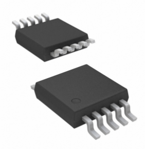
Available Packages: QFN1.8×1.4-10L, DFN3x3-10L, and MSOP-10L
PIN CONFIGURATION (Top View)
NC2 GND
IN2
8
COM2
NO2
7
6
5
NC1
9
4
IN1
10
3
COM1
XCC
1
10
No2
NO1
2
9
COM2
COM1
3
8
IN2
1
1
IN1
4
7
NC2
VCC
NO1
NC1
5
6
GND
QFN 1.8 X 1.4-10L
DFN 3 X 3-10L
XCC
1
10
No2
NO1
2
9
COM2
COM1
3
8
IN2
IN1
4
7
NC2
NC1
5
6
GND
MSOP-10L
CAUTION: These devices are sensitive to electrostatic discharge; follow proper IC Handling Procedures.
Linearin and designs are registered trademarks of Linearin Technology Corporation.
© Copyright Linearin Technology Corporation. All Rights Reserved.
All other trademarks mentioned are the property of their respective owners.
FN1620-22.1 — Data Sheet
Ultra-Low 0.5Ω Dual SPDT Analog Switch
�LTC5223
P-2
ORDER INFORMATION
Model
LTC5223
Package
Ordering Number
Packing Option
QFN1.8×1.4-10L
LTC5223YFS10
Tape and Reel, 3 000
DFN3×3-10L
LTC5223YF10
Tape and Reel, 3 000
MSOP-10L
LTC5223YV10
Tape and Reel, 4 000
PIN DESCRIPTIONS
Pin
Symbol
Description
1
VCC
Power Supply
2
NO1
Independent Channels
3
COM1
Common Channels
4
IN1
Controls
5
NC1
Independent Channels
6
GND
Ground (V)
7
NC2
Independent Channels
8
IN2
Controls
9
COM2
Common Channels
10
NO2
Independent Channels
TRUTH TABLE
IN1, IN2
NO1, NO2
NC1, NC2
0
OFF
ON
1
ON
OFF
CAUTION: These devices are sensitive to electrostatic discharge; follow proper IC Handling Procedures.
Linearin and designs are registered trademarks of Linearin Technology Corporation.
© Copyright Linearin Technology Corporation. All Rights Reserved.
All other trademarks mentioned are the property of their respective owners.
FN1620-22.1 — Data Sheet
Ultra-Low 0.5Ω Dual SPDT Analog Switch
�LTC5223
P-3
RECOMMENDED OPERATING CONDITIONS
Characteristic
Symbol
Min
Max
Unit
DC Supply Voltag
VCC
1.65
5.5
V
Digital Select Input Voltage
VIN
GND
5.5
V
Analog Input Voltage
VIS
GND
VCC
V
Operating Temperature Range
TA
-45
+85
℃
0
20
0
10
Input Rise or Fall Time
SELECT
VCC = 1.6 V to 2.7 V
VCC = 3.0 V to 5.5 V
tR, tF
ns/V
ABSOLUTE MAXIIMUM RATINGS
Characteristic
Symbol
Value
Unit
Supply Voltage
VCC
-0.5 to 6.0
V
Analog Input Voltage
VIS
-0.5 to VCC + 0.5
V
Digital Select Input Voltage
VIN
-0.5 to 6.0
V
Output Voltage
VOUT
-0.5 to VCC + 0.5
V
Continuous DC Current from COM to NC/NO
Ian1
±300
mA
Ian1-pk1
±500
mA
Iclmp
±100
mA
Peak Current from COM to NC/NO,
10 duty cycle (Note 1)
Continuous DC Current into COM/NO/NC with
respect to VCC or GND
Stresses beyond those listed under “Absolute Maximum Ratings” may cause permanent damage to the device.
These are stress ratings only, and functional operation of the device at these or any other conditions beyond
those indicated in the operational sections of the specifications is not implied. Exposure to absolute maximum
rating conditions for extended periods may affect device reliability.
Note 1. Defined as 10% ON, 90% off duty cycle.
CAUTION
This integrated circuit can be damaged by ESD if you don’t pay attention to ESD protection. Lineaein
recommends that all integrated circuits be handled with appropriate precautions. Failure to observe proper
handling and installation procedures can cause damage. ESD damage can range from subtle performance
degradation to complete device failure. Precision integrated circuits may be more susceptible to damage
because very small parametric changes could cause the device not to meet its published specifications.
Linearin reserves the right to make any change in circuit design, specification or other related things if
necessary without notice at any time. Please contact Linearin sales office to get the latest data sheet.
CAUTION: These devices are sensitive to electrostatic discharge; follow proper IC Handling Procedures.
Linearin and designs are registered trademarks of Linearin Technology Corporation.
© Copyright Linearin Technology Corporation. All Rights Reserved.
All other trademarks mentioned are the property of their respective owners.
FN1620-22.1 — Data Sheet
Ultra-Low 0.5Ω Dual SPDT Analog Switch
�LTC5223
P-4
ELECTRICAL CHARACTERISTICS (DC)
Symbol Parameter
VIH
VIL
Test Conditions
High-Level Input Voltage,
Select Inputs
Low−Level Input Voltage,
Select Inputs
VCC ± 10%
TA = 25℃
Min
Typ
Max
TA = –40
to +85℃
Min Max
1.65 ~ 1.95 1.1
1.1
2.3 ~ 2.5
1.2
1.2
2.7 ~ 3.0
1.3
1.3
3.0 ~ 3.6
1.4
1.4
4.3
1.5
Unit
V
1.5
1.65 ~ 1.95
0.25
0.25
2.3 ~ 2.5
0.25
0.25
2.7 ~ 3.0
0.25
0.25
3.0 ~ 3.6
0.30
0.30
4.3
0.40
0.40
V
IIN
Maximum Input Leakage
Current, Select Inputs
VIN =VCC or GND
4.3
±0.1
±1.0
μA
IOFF
Power Off Leakage
Current
VIN =VCC or GND
0
±0.5
±2.0
μA
ICC
Maximum Quiescent
Supply Current (Note 2)
Select,
VIS = VCC or GND
1.65 ~ 4.3
±1.0
±2.0
μA
INO (OFF)
INC (OFF)
NC or NO Off
Leakage
Current
VIN = VIL or VIH
VNO or VNC = 0.3 V
VCOM = 4.0 V
10
nA
4.3
-5.0
5.0
-10
4.3
-10
10
-100 100
COM ON Leakage Current (Note 3)
ICOM (ON)
RON
RFLAT
∆RON
VIN = VIL or VIH, VNO = 0.3 V or 4.0 V
VNC floating VNC = 0.3 V or 4.0 V
VNO floating VCOM = 0.3 V or 4.0 V
OnResistance
(Note 3)
On−Resistance Flatness
(Note 3) (Note 5)
On-Resistance Match
Between Channels
(Note 3) (Note 4)
VIS = GND to VCC,
IIN = 100 mA
ICOM = 100 mA
VIS = 1.5 V
ICOM = 100 mA
VIS = 1.5 V
4.3
0.45
0.5
0.55
3.6
0.5
0.55
0.65
3.0
0.5
0.55
0.65
2.7
0.6
0.7
0.8
2.3
0.6
0.7
0.8
1.8
0.9
1.0
1.1
4.3
0.15
0.20
0.20
3.6
0.15
0.20
0.20
3.0
0.15
0.20
0.20
2.7
0.15
0.20
0.20
2.3
0.20
0.25
0.25
1.8
0.35
0.45
0.45
2.7
0.1
CAUTION: These devices are sensitive to electrostatic discharge; follow proper IC Handling Procedures.
Linearin and designs are registered trademarks of Linearin Technology Corporation.
© Copyright Linearin Technology Corporation. All Rights Reserved.
All other trademarks mentioned are the property of their respective owners.
nA
Ω
Ω
Ω
FN1620-22.1 — Data Sheet
Ultra-Low 0.5Ω Dual SPDT Analog Switch
�LTC5223
P-5
ELECTRICAL CHARACTERISTICS (AC)
Symbol
Parameter
tPLH
tPHL
Propagation Delay
tON
Turn−On Time
(Figure 1)
Test Conditions
VIS = 0.8 V
VIS = 1.5 V
VIS = 0.8 V
tOFF
tBBM
BW
Turn−Off Time
(Figure 1)
VIS = 1.5 V
Break-Before-MakeTime
(Note6)( Figure 2)
CL= 35 pF
RIS = 50 Ω
VIS = 1.5 V
On-Channel, -3 dB Bandwidth or Frequency
Response (Figure 4)
VCC ± 10%
1.65 ~ 1.95
2.3 ~ 2.7
3.0 ~ 3.3
3.6 ~ 5
1.65 ~ 1.95
2.3 ~ 2.7
3.0 ~ 3.3
3.6 ~ 4.3
1.65 ~ 1.95
2.3 ~ 2.7
3.0 ~ 3.3
3.6 ~ 4.3
1.65 ~ 1.95
2.3 ~ 2.7
3.0 ~ 3.3
3.6 ~ 4.3
Min
2
2
2
2
TA = 25℃
Typ
Max
0.30
0.25
0.20
0.20
120
65
85
42
55
40
55
45
18
30
16
30
15
30
17
10
8
7
Unit
ns
ns
ns
ns
1.65 ~ 4.3
18
MHz
FIS = 100 kHz, VIN = GND to VCC, CL = 5 pF
RL = 50 Ω, VIS = 1VRMS
1.65 ~ 4.3
-66
dB
Charge Injection Select Input to Common I/O
(Figure 3)
1.65 ~ 1.95
43
2.3 ~ 2.7
3.0 ~ 3.3
3.6 ~ 4.3
51
51
49
pC
3.0
0.08
%
1.65 ~ 4.3
-72
dB
RIS = 50 Ω
Off-Channel Isolation (Figure 4)
VISO
Q
VIN = 0 or VCC, RIS = 0 Ω, CL = 100 pF
RL = 1 mΩ, Q = CL × ∆VOUT
Total Harmonic Distortion THD +Noise
THD
FIS = 20 Hz to 20 kHz, RL = 600 Ω
CL = 50 pF VIS = 2 VRMS
Channel - to - Channel Crosstalk (Figure 4)
VCT
FIS = 100 kHz, VIN = GND to VCC
RL = 50 Ω, CL = 5 pF, VIS = 1 VRMS
CIN
Control Pin Input Capacitance
3.6
3.5
pF
CCN/CNO
NC/NO Port Capacitance
3.6
60
pF
CCOM
COM Port Capacitance
When Switch is Enabled
3.6
200
pF
Note:
2. Guaranteed by design.
3. Guaranteed by design. Resistance measurements do not include test circuit or package resistance.
4. ∆RON = RON (MAX) − RON (MIN) between NC1 and NC2 or between NO1 and NO2.
5. Flatness is defined as the difference between the maximum and minimum value of on−resistance as
measured over the specified analog signal ranges.
6. Guaranteed by design in -40℃.
CAUTION: These devices are sensitive to electrostatic discharge; follow proper IC Handling Procedures.
Linearin and designs are registered trademarks of Linearin Technology Corporation.
© Copyright Linearin Technology Corporation. All Rights Reserved.
All other trademarks mentioned are the property of their respective owners.
FN1620-22.1 — Data Sheet
Ultra-Low 0.5Ω Dual SPDT Analog Switch
�LTC5223
P-6
TEST CIRCUITS
DUT
VCC
0.1μF
Output
VOUT
Open
50Ω
35pF
Input
DUT
VCC
0.1μF
Output
VOUT
Open
50Ω
35pF
Input
Figure 1. tON/tOFF
DUT
VCC
Output
0.1μF
VOUT
50Ω
35pF
Swith Select Pin
Figure 2. tBBM
DUT
Open
Output
CL
VIN
Figure3: Charge Injection
CAUTION: These devices are sensitive to electrostatic discharge; follow proper IC Handling Procedures.
Linearin and designs are registered trademarks of Linearin Technology Corporation.
© Copyright Linearin Technology Corporation. All Rights Reserved.
All other trademarks mentioned are the property of their respective owners.
FN1620-22.1 — Data Sheet
Ultra-Low 0.5Ω Dual SPDT Analog Switch
�LTC5223
P-7
TEST CIRCUITS (Cont.)
Reference
50Ω
DUT
Input
Output
Transmitted
50Ω Generator
50Ω
VISO = 20log (VOUT/VIN)
VONL = 20log (VOUT/VIN)
VCT = 20log (VOUT/VIN)
BW = the frequency 3dB below V ONL
Figure 4. -3dB Bandwidth/Off Channel Isolation/On Channel
Loss(BW)/Crosstalk (On Channel to Off Channel)/V ONL
TEST CIRCUITS (Cont.)
CAUTION: These devices are sensitive to electrostatic discharge; follow proper IC Handling Procedures.
Linearin and designs are registered trademarks of Linearin Technology Corporation.
© Copyright Linearin Technology Corporation. All Rights Reserved.
All other trademarks mentioned are the property of their respective owners.
FN1620-22.1 — Data Sheet
Ultra-Low 0.5Ω Dual SPDT Analog Switch
�LTC5223
P-8
PACKAGE OUTLINE
QFN1.8×1.4-10L
PIN 1 DOT
BY MARKING
b
D
L1
PIN 1 IDENTIFICATION
CHAMFER
L
E
e
TOP VIEW
BOTTOM VIEW
A
A1
A3
SIDE VIEW
Dimensions In Millimeters (mm)
Symbol
Min.
Nom.
Max.
A
0.500
0.550
0.600
A1
0.000
A3
0.050
0.15 REF
D
1.350
1.400
1.450
E
1.750
1.800
1.850
b
0.150
0.200
0.250
L
0.300
0.400
0.500
L1
0.400
0.500
0.600
e
0.40 BSC
CAUTION: These devices are sensitive to electrostatic discharge; follow proper IC Handling Procedures.
Linearin and designs are registered trademarks of Linearin Technology Corporation.
© Copyright Linearin Technology Corporation. All Rights Reserved.
All other trademarks mentioned are the property of their respective owners.
FN1620-22.1 — Data Sheet
Ultra-Low 0.5Ω Dual SPDT Analog Switch
�LTC5223
P-9
PACKAGE OUTLINE
DFN3×3-10L
b
D
L1
k
R
E
D2
(C=0.25)
E2
LASER MARK
L
TOP VIEW
e
BOTTOM VIEW
A
A1
A3
SIDE VIEW
Symbol
A
A1
A3
b
D
D2
e
E
E2
L
k
R
Dimensions In Millimeters (mm)
Min.
Max.
0.700
0.800
0.000
0.050
0.203REF
0.180
0.300
2.900
3.100
2.450
2.550
0.400
0.600
2.900
3.100
1.450
1.650
0.350
0.450
0.150
0.090
CAUTION: These devices are sensitive to electrostatic discharge; follow proper IC Handling Procedures.
Linearin and designs are registered trademarks of Linearin Technology Corporation.
© Copyright Linearin Technology Corporation. All Rights Reserved.
All other trademarks mentioned are the property of their respective owners.
b
FN1620-22.1 — Data Sheet
Ultra-Low 0.5Ω Dual SPDT Analog Switch
�LTC5223
P-10
PACKAGE OUTLINE
MSOP-10L
θ
H
C2
B1
B
C3
C4
B2
A1
A2
A3
R
A
θ2
C1
θ3
R1
C
θ
Symbol
A
A1
A2
A3
B
B1
B2
C
C1
C2
Dimensions In Millimeters (mm)
Min.
2.900
0.190
0.500 TYP
0.400 TYP
2.900
4.700
0.450
0.750
0.328 TYP
CAUTION: These devices are sensitive to electrostatic discharge; follow proper IC Handling Procedures.
Linearin and designs are registered trademarks of Linearin Technology Corporation.
© Copyright Linearin Technology Corporation. All Rights Reserved.
All other trademarks mentioned are the property of their respective owners.
Max.
3.100
0.280
3.100
5.100
0.750
0.950
1.100
FN1620-22.1 — Data Sheet
Ultra-Low 0.5Ω Dual SPDT Analog Switch
�
很抱歉,暂时无法提供与“LTC5223YV10”相匹配的价格&库存,您可以联系我们找货
免费人工找货- 国内价格
- 1+3.60720
- 10+2.90520
- 30+2.55960