LTP3559A
P-1
General Description
The LTP3559A is a high voltage, low power consumption and high performance LDO. The family
uses an advanced CMOS process and a P-MOSFET pass device to achieve fast start-up, with high
output voltage accuracy. The LTP3559A is stable with a 1.0μF~10μF ceramic output capacitor, and
uses a precision voltage reference and feedback loop to achieve a worst-case accuracy of 1% over
all load, line, process, and temperature variations.
Features
◼
◼
◼
◼
◼
◼
◼
◼
◼
◼
Wide Input Voltage Range : up to 45V
Output Current : 350mA
Standard Fixed Output Voltage Options : 3.3V, 5.0V
More Output Voltage Options Available on Request
Low IQ : 2.6 μA Typically
Low Dropout Voltage
Short current protection:150mA
Excellent Load and Line Transient Response
Line Regulation : 0.01%/V Typically
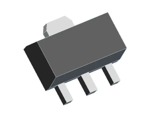
Package: SOT89-3
Order Information
Model
LTP3559A
Package
Ordering Number Note1
Packing Option
SOT89-3
LTP3559A-33XT4
Tape and Reel, 1000
SOT89-3
LTP3559A-50XT4
Tape and Reel, 1000
SOT89-3
LTP3559A-33RXT4
Tape and Reel, 1000
SOT89-3
LTP3559A-50RXT4
Tape and Reel, 1000
CAUTION: These devices are sensitive to electrostatic discharge; follow proper IC Handling Procedures.
Linearin and designs are registered trademarks of Linearin Technology Corporation.
© Copyright Linearin Technology Corporation. All Rights Reserved.
All other trademarks mentioned are the property of their respective owners.
FN1622-12.1 — Data Sheet
350-mA, 45-V, Ultra-Low IQ , Low Dropout LDOs
�LTP3559A
P-2
Pin Description
Top View
1
GND
2
IN
1
OUT
3
OUT
2
GND
3
IN
SOT89-3
SOT89-3
Pin Function
Pin No.
SOT89-3
SOT89-3
LTP3559A-xxXT4
LTP3559A-xxRXT4
1
Pin Name
Pin Function
2
GND
Ground.
2
3
IN
Supply input pin.
3
1
OUT
Output pin.
CAUTION: These devices are sensitive to electrostatic discharge; follow proper IC Handling Procedures.
Linearin and designs are registered trademarks of Linearin Technology Corporation.
© Copyright Linearin Technology Corporation. All Rights Reserved.
All other trademarks mentioned are the property of their respective owners.
FN1622-12.1 — Data Sheet
350-mA, 45-V, Ultra-Low IQ , Low Dropout LDOs
�LTP3559A
P-3
Block Diagram
OUT
IN
Short
Current protection
+
Voltage
Reference
GND
Functional Description
Input Capacitor
A 1μF-10μF ceramic capacitor is recommended to connect between VIN and GND pins to decouple input power
supply glitch and noise. The amount of the capacitance may be increased without limit. This input capacitor
must be located as close as possible to the device to assure input stability and less noise. For PCB layout, a
wide copper trace is required for both VIN and GND.
Output Capacitor
An output capacitor is required for the stability of the LDO. The recommended output capacitance is from
1μF to 10μF, Equivalent Series Resistance (ESR) is from 5mΩ to 100mΩ, and temperature characteristics
are X7R or X5R. Higher capacitance values help to improve load/line transient response. The output
capacitance may be increased to keep low undershoot/overshoot. Place output capacitor as close as
possible to OUT and GND pins.
Low Quiescent Current
The LTP3559A, consuming only around 2.6μA for all input range and output loading, provides great power
saving in portable and low power applications.
Short Current Limit Protection
When output current at the OUT pin is higher than current limit threshold or the OUT pin is short-circuit to
GND, the short current limit protection will be triggered and clamp the output current to approximately
150mA to prevent over-current and to protect the regulator from damage due to overheating.
CAUTION: These devices are sensitive to electrostatic discharge; follow proper IC Handling Procedures.
Linearin and designs are registered trademarks of Linearin Technology Corporation.
© Copyright Linearin Technology Corporation. All Rights Reserved.
All other trademarks mentioned are the property of their respective owners.
FN1622-12.1 — Data Sheet
350-mA, 45-V, Ultra-Low IQ , Low Dropout LDOs
�P-4
LTP3559A
Absolute Maximum Ratings
Parameter
Rating
Unit
–0.3 to 48
V
–0.3 to 6
V
135
℃/W
Operating Junction Temperature
–40 to 125
℃
Storage Temperature
–65 to 150
℃
IN pin to GND pin
OUT pin to GND pin
Thermal Resistance (Junction to Ambient)
Lead Temperature (Soldering, 10 sec)
ESD (HBM mode) ESDA/JEDEC JS-001-2017
300
±2000V
℃
V
Stresses exceeding those listed in the Maximum Ratings table may damage the device. If any of these limits
are exceeded, device functionality should not be assumed, damage may occur and reliability may be
affected.
CAUTION: These devices are sensitive to electrostatic discharge; follow proper IC Handling Procedures.
Linearin and designs are registered trademarks of Linearin Technology Corporation.
© Copyright Linearin Technology Corporation. All Rights Reserved.
All other trademarks mentioned are the property of their respective owners.
04
FN1622-12.1 — Data Sheet
350-mA, 45-V, Ultra-Low IQ , Low Dropout LDOs
�LTP3559A
P-5
Electrical Characteristics
(VIN = VOUT + 2V; IOUT = 10mA, CIN = COUT = 1.0μF, unless otherwise noted. Typical values are at T A = +25°C.)
Symbol
Parameter
Test Conditions
VIN
Operating Input Voltage
VOUT
Regulated Output Voltage
IOUT=1mA
LineREG
Line Regulation
2.5V ≤ VIN ≤36V,
IOUT = 10mA
0.01
VDROP
Dropout Voltage
VOUT= 3.3V, IOUT = 100mA
330
VOUT= 3.3V, IOUT = 200mA
690
LoadREG
Load Regulation
1mA ≤ IOUT ≤ 300mA,
VIN =VOUT+2V
IOUT
Maximum Output Current
VIN = VOUT +2V
IQ
Quiescent Current
IOUT = 0mA
2.6
PSRR
Power Supply Rejection Ratio
VIN = VOUT+1V , IOUT = 20mA
f = 1 kHz
60
dB
eN
Output Noise Voltage
VIN = VOUT+2V, IOUT = 1mA,
f = 10Hz to 100KHz,
(VOUT =3.3V) COUT = 1μF
100
μVrms
TSD
Thermal Shutdown
Temperature
Temperature Increasing
from TA=+25°C
155
℃
TSDH
Thermal Shutdown
Hysteresis
Temperature Falling
From TSD
20
℃
CAUTION: These devices are sensitive to electrostatic discharge; follow proper IC Handling Procedures.
Linearin and designs are registered trademarks of Linearin Technology Corporation.
© Copyright Linearin Technology Corporation. All Rights Reserved.
All other trademarks mentioned are the property of their respective owners.
Min
Typ
VOUT
X 0.99
Max
Unit
45
V
VOUT
X 1.01
V
0.04
%/V
mV
40
350
mV
mA
4
μA
FN1622-12.1 — Data Sheet
350-mA, 45-V, Ultra-Low IQ , Low Dropout LDOs
�P-6
LTP3559A
TYPICAL PERFORMANCE CHARACTERISTICS
Fig1. Line-Transient Response
Fig2. Load-Transient Response
Fig3. Start up Response
CAUTION: These devices are sensitive to electrostatic discharge; follow proper IC Handling Procedures.
Linearin and designs are registered trademarks of Linearin Technology Corporation.
© Copyright Linearin Technology Corporation. All Rights Reserved.
All other trademarks mentioned are the property of their respective owners.
06
FN1622-12.1 — Data Sheet
350-mA, 45-V, Ultra-Low IQ , Low Dropout LDOs
�LTP3559A
P-7
IQ vs. Temperature
VDROP VS. IOUT
3.5
1000
IQ (μA)
Dropout Voltage(mV)
3.2
100
2.9
2.6
10
2.3
2
1
0
50
100
150
200
250
300
-40 -20
350
0
20
40
60
80
100 120
Temperature(℃)
Output Current (mA)
Fig5. IQ VS Temperature
Fig4. Dropout Voltage VS Output Current
Application Circuits
VIN
IN
OUT
VOUT
CIN
COUT
1µF
1µF
GND
CAUTION: These devices are sensitive to electrostatic discharge; follow proper IC Handling Procedures.
Linearin and designs are registered trademarks of Linearin Technology Corporation.
© Copyright Linearin Technology Corporation. All Rights Reserved.
All other trademarks mentioned are the property of their respective owners.
FN1622-12.1 — Data Sheet
350-mA, 45-V, Ultra-Low IQ , Low Dropout LDOs
�LTP3559A
P-8
Package Dimension
SOT89-3/ SOT89-3R
4.4~4.6
1.4~1.6
0.9~1.2
2.3~2.6
3.94~4.25
1.55
1.50
0.32~0.52
3.00
CAUTION: These devices are sensitive to electrostatic discharge; follow proper IC Handling Procedures.
Linearin and designs are registered trademarks of Linearin Technology Corporation.
© Copyright Linearin Technology Corporation. All Rights Reserved.
All other trademarks mentioned are the property of their respective owners.
0.35~0.44
Unit:mm
08
FN1622-12.1 — Data Sheet
350-mA, 45-V, Ultra-Low IQ , Low Dropout LDOs
�