www.msksemi.com
�RCLAMP0521P.TCT
Semiconductor
Compiance
Features
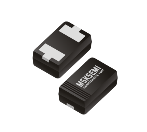
PIN CONFIGURATION
■
100Watts peak pulse power (tp = 8/20μs)
■
Tiny DFN1006 package
■
Bidirectional configurations
■
Solid-state silicon-avalanche technology
■
Low clamping voltage
■
Low leakage current
■
Low capacitance (Cj=0.25pF typ. IO to
IO)
■
Protection one data/power line to:
■
IEC 61000-4-2 ±20kV contact ±20kV air
■
IEC 61000-4-4 (EFT) 40A (5/50ns)
■
IEC 61000-4-5 (Lightning) 4A (8/20μs)
Applications
0402
■
Cell Phone Handsets and Accessories
■
Microprocessor based equipment
■
Personal Digital Assistants (PDA’s)
■
Notebooks, Desktops, and Servers
■
Portable Instrumentation
Mechanical Data
■
0402
■
Molding compound flammability rating: UL 94V-0
■
Packaging: Tape and Reel
■
RoHS/WEEE Compliant
Electrical Parameters (TA = 25°C unless otherwise noted)
Symbol
Parameter
IPP
Maximum Reverse Peak Pulse Current
VC
Clamping Voltage @ IPP
VRWM
IR
VBR
IT
I
IPP
Working Peak Reverse Voltage
Maximum Reverse Leakage Current @ VRWM
VC VBR
VRWM
IT
IR
I
IT R
VRWM
VBR VC
V
Breakdown Voltage @ IT
Test Current
IPP
Note:. 8/20μs pulse waveform.
www.msksemi.com
�RCLAMP0521P.TCT
Semiconductor
Compiance
Absolute Maximum Rating
Rating
Symbol
Value
Units
Peak Pulse Power ( tp =8/20μs )
PPP
100
Watts
Peak Pulse Current ( tp =8/20μs ) (note1)
Ipp
4.0
A
VESD
20
20
kV
Lead Soldering Temperature
TL
260(10seconds)
℃
Junction Temperature
TJ
-55 to + 125
℃
Storage Temperature
Tstg
-55 to + 125
℃
ESD per IEC 61000-4-2 (Air)
ESD per IEC 61000-4-2 (Contact)
Electrical Characteristics
Parameter
Reverse Stand-Off Voltage
Reverse Breakdown Voltage
Symbol
Conditions
Min
Typical
VRWM
VBR
IT=1mA
Reverse Leakage Current
IR
VRWM=5V,T=25℃
Peak Pulse Current
IPP
tp =8/20μs
Clamping Voltage
VC
IPP=4A,tp=8/20μs
Junction Capacitance
Cj
IO to IO
VR = 0V, f = 1MHz
Max
Units
5.0
V
6.0
V
0.25
100
nA
4.0
A
25
V
0.4
pF
www.msksemi.com
�RCLAMP0521P.TCT
Semiconductor
Typical
Characteristics
Figure 2: Power Derating Curve
110
10
Percent of Rated Power for Ipp
Ppp – Peak Pulse Power - Ppp(KW)
Figure 1: Peak Pulse Power vs. Pulse Time
1
100w 8/20µswaveform
0.1
0.01
0.1
1
10
90
80
70
60
50
40
30
20
10
0
1,000
100
100
0
25
td – Pulse Duration - µs
80
Ipp
125
150
26
Clamping Voltage–VC (V)
90
Percent
100
20
Waveform
Paramters
tr=8µs
td=20µs
100
70
e
75
Figure 4: Clamping Voltage vs.Ipp
110
60
50
Ambient Temperature - TA (℃)
Figure3: Pulse Waveform
-1
50
40
30
td=Ipp/2
20
23
20
17
Test
Waveform
Paramters
tr=8µs
td=20µs
14
11
8
5
10
0
2
0
5
10
15
20
25
30
0
Time (µs)
IPP
(A)
Compiance
1
2
3
4
5
6
Peak Pulse Current–IPP (A)
Figure5: Positive Clamping voltage (TLP)
Figure5: Negative Clamping voltage (TLP)
35
0
30
5
25
10
20
IPP
(A)
15
Rdyn = 0.55 Ω
20
15
Rdyn = 0.55 Ω
10
25
5
30
0
-0.5
35
4.5
9.5
14.5
19.5
24.5
VCL (V)
-24.5
-19.5
-14.5
-9.5
-4.5
0.5
VCL (V)
www.msksemi.com
�RCLAMP0521P.TCT
Semiconductor
Compiance
PACKAGE MECHANICAL DATA
A
Dim
B
C
R
E
D
Millimeters
MIN
MAX
MIN
MAX
A
0.0125
0.02
0.32
0.52
B
0.000
0.002
0.00
0.05
C
0.037
0.043
0.95
1.080
D
0.022
0.027
0.55
0.680
E
0.016
0.024
0.40
0.60
F
0.008
0.012
0.20
0.30
H
R
F
Inches
0.015Typ.
0.001
0.40Typ.
0.005
0.05
0.15
H
1.20
0.50
0.60
0.70
NOTES:
1. CONTROLLING DIMENSIONS ARE IN MILLIMETERS (ANGLES IN DEGREES).
2. THIS LAND PATTERN IS FOR REFERENCE PURPOSES ONLY.
CONSULT YOUR MANUFACTURING GROUP TO ENSURE YOUR
COMPANY'S MANUFACTURING GUIDELINES ARE MET.
REEL SPECIFICATION
P/N
RCLAMP0521P.TCT
PKG
QTY
0402
10000
www.msksemi.com
�RCLAMP0521P.TCT
Semiconductor
Compiance
Attention
■ Any and all MSKSEMI Semiconductor products described or contained herein do not have specifications
that can handle applications that require extremely high levels of reliability, such as life-support systems,
aircraft's control systems, or other applications whose failure can be reasonably expected to result in serious
physical and/or material damage. Consult with your MSKSEMI Semiconductor representative nearest you
before using any MSKSEMI Semiconductor products described or contained herein in such applications.
■ MSKSEMI Semiconductor assumes no responsibility for equipment failures that result from using products
at values that exceed, even momentarily, rated values (such as maximum ratings, operating condition ranges, or
other parameters) listed in products specificationsof any andall MSKSEMI Semiconductor products described
orcontained herein.
■ Specifications of any and all MSKSEMI Semiconductor products described or contained herein stipulate the
performance, characteristics, and functions of the described products in the independent state, and are not
guarantees of the performance, characteristics, and functions of the described products as mounted in the
customer’s products or equipment. To verify symptoms and states that cannot be evaluated in an independent
device, the customer should always evaluate and test devices mounted in the customer’sproducts orequipment.
■ MSKSEMI Semiconductor. strives to supply high-quality high-reliability products. However, any and all
semiconductor products fail with someprobability. It is possiblethat these probabilistic failures could give rise to
accidents or events that could endanger human lives, that could give rise to smoke or fire, or that could cause
damage to other property. When designing equipment, adopt safety measures so that these kinds of accidents
or events cannot occur. Such measures include but are not limited to protective circuits anderror prevention
circuitsfor safedesign, redundant design, and structural design.
■ In the event that any or all MSKSEMI Semiconductor products(including technical data, services) described
or contained herein are controlled under any of applicable local export control laws and regulations, such
products must not be exported without obtaining the export license from theauthorities concerned in
accordance with the above law.
■ No part of this publication may be reproduced or transmitted in any form or by any means, electronic or
mechanical, including photocopying and recording, or any information storage or retrieval system, or otherwise,
without the prior written permission of MSKSEMI Semiconductor.
■ Information (including circuit diagrams and circuit parameters) herein is for example only ; it is not
guaranteed for volume production. MSKSEMI Semiconductor believes information herein is accurate and
reliable, but no guarantees are made or implied regarding its use or any infringementsof intellectual property
rights or other rightsof third parties.
■ Any and all information described or contained herein are subject to change without notice due to
product/technology improvement, etc. Whendesigning equipment, referto the "Delivery Specification" for the
MSKSEMI Semiconductor productthat you intend to use.
www.msksemi.com
�
很抱歉,暂时无法提供与“RCLAMP0521P.TCT”相匹配的价格&库存,您可以联系我们找货
免费人工找货