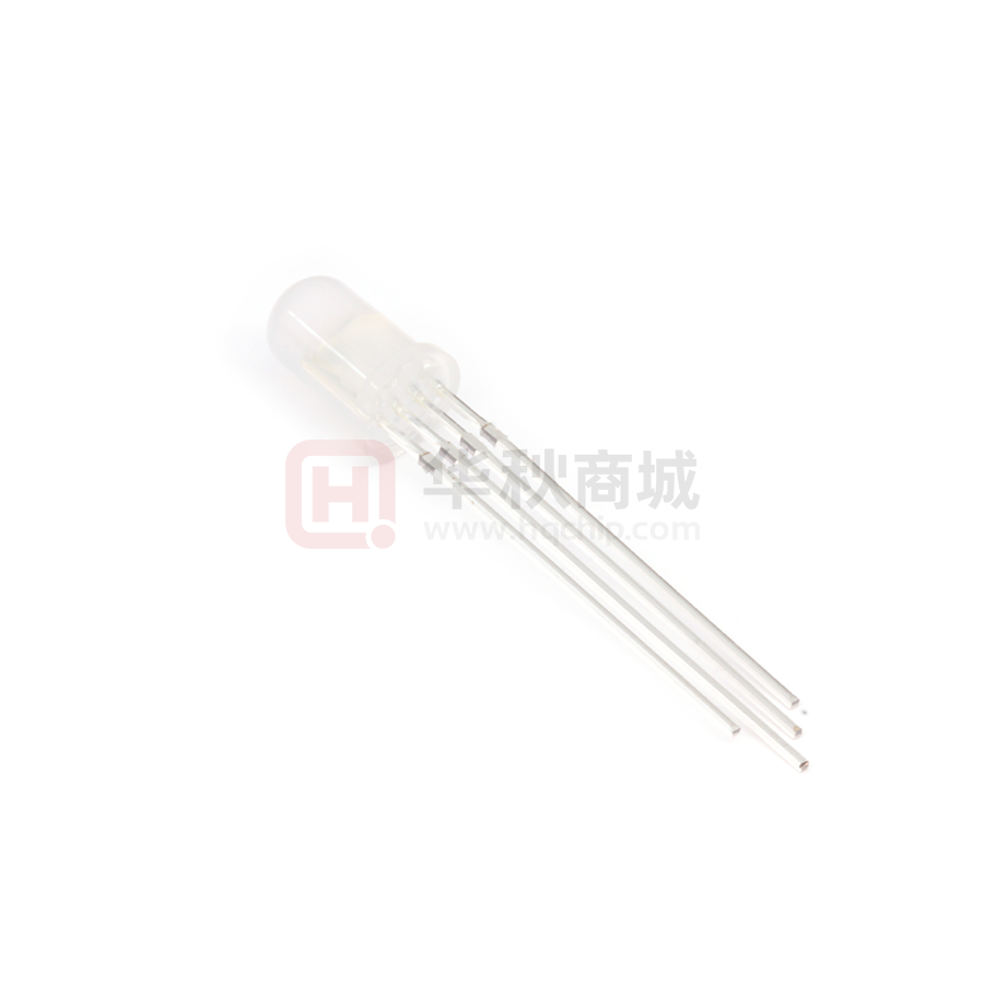
WS2812D-F5-1261
Intelligent control LED
integrated light source
Features and Benefits
The control circuit and the LED share the only power source.
Control circuit and RGB chip are integrated in a package of F5 plug-in components, to form a complete addressable
pixel.
Built-in signal reshaping circuit, after wave reshaping to the next driver, ensure wave-form distortion not
accumulate.
Built-in electric reset circuit and power lost reset circuit.
Each pixel of the three primary color can achieve 256 brightness display, completed 16777216 color full color
display, and scan frequency is of 2KHz.
Cascading port transmission signal by single line.
When the refresh rate is 30fps, cascade number are not less than 1024 pixels.
Send data at speeds of 800Kbps.
The color of the light is highly consistent, cost-effective.
Reverse-connection protection.
Applications
Full-color module, LED full-color soft/hard light bar, LED guardrail tube.
LED decorative lighting, LED Screen, Indoor/outdoor LED video irregular screen, various electronic products,
electrical equipment marquee.
General description
WS2812D-F5-1261 is an intelligent external control LED light source that integrates control circuit and
light-emitting circuit. Its appearance is the same as an F5 LED lamp bead, and each element is a pixel.It internal include
intelligent digital port data latch and signal reshaping amplification drive circuit.Also include a precision internal
oscillator and a voltage programmable constant current control part, effectively ensuring the pixel point light color height
consistent.
The data transfer protocol use single NZR communication mode. After the pixel power-on reset, the DIN port
receive data from controller, the first pixel collect initial 24bit data then sent to the internal data latch, the other data
which reshaping by the internal signal reshaping amplification circuit sent to the next cascade pixel through the DO port.
After transmission for each pixel, the signal to reduce 24bit. pixel adopt auto reshaping transmit technology, making the
pixel cascade number is not limited the signal transmission, only depend on the speed of signal transmission.
LED with low driving voltage, environmental protection and energy saving, high brightness, scattering angle is
large, good consistency, low power, long life and other advantages. The control chip integrated in LED above becoming
more simple circuit, small volume, convenient installation.
1
http://www.world-semi.com
�WS2812D-F5-1261
Intelligent control LED
integrated light source
Mechanical Dimensions(Unit:mm)
PIN Function
NO. Symbol
PIN
Function description
1
Dout
DATA OUT
Control data signal output
2
VCC
POWER SUPPLY
3
GND
GROUND
Ground,data & power grounding
4
Din
DATA IN
Control data signal input
Power supply
Absolute Maximum Ratings(TA=25℃, VCC=5V, VSS=0V, unless otherwise specified)
Parameter
Symbol
Ratings
Unit
Power supply voltage
Vcc
+3.7~+5.3
V
Logical Input Voltage
VI
-0.3V~VCC+0.7V
V
Operation junction temperature
Topt
-25~+85
℃
Storage temperature range
Tstg
-40~+105
℃
2
http://www.world-semi.com
�WS2812D-F5-1261
Intelligent control LED
integrated light source
Electrical Characteristics(TA=-20~+70℃,VCC=5V,VSS=0V,unless otherwise specified)
Parameter
Symbol
Min
Tpy
Max
Unit
Conditions
RGB Current
Iout
32
36
40
mA
R+G+B
Input current
II
——
——
±1
µA
VI=VCC/VSS
High Voltage Input
VIH
2.7V
——
VCC+0.7V
V
DIN
Low Voltage Input
VIL
-0.3V
——
0.7V
V
DIN
Switching Characteristics(TA=-20~+70℃,VCC=5V,VSS=0V,unless otherwise specified)
Parameter
Symbol Min Tpy Max Unit
Condition
Oscillation frequency
Fosc
——
800
——
KHz
——
Transmission delay
time
tPLZ
——
——
300
ns
CL=15pF, DIN→DOUT, RL=10KΩ
Fall time
tTHZ
——
——
120
µs
CL=300pF, OUTR/OUTG/OUTB
Input capacity
CI
——
——
15
pF
——
LED light chip parameters
Quiescent Current: 0.6mA
Parameter
Brightness
Wavelength
Symbol
IV
λd
Color
Mini
Typ
Max
Red
250
--
350
Green
500
--
700
Blue
80
--
150
Red
620
--
625
Green
520
--
530
Blue
465
--
475
Unit
mcd
nm
Sequence waveform
Sequence Chart
Cascade Method
D1
DIN DO
PIX1
3
http://www.world-semi.com
D2
DIN DO
PIX2
D3
DIN DO
PIX3
D4
�WS2812D-F5-1261
Intelligent control LED
integrated light source
Data Transfer Time:
0 code, high voltage time
220ns~380ns
T1H
1 code, high voltage time
580ns~1µs
T0L
0 code, low voltage time
580ns~1µs
T1L
1 code, low voltage time
580ns~1µs
RES
Frame unit, low voltage time
>280µs
Title
T0H
Data Transmission Method
Note: The data of D1 is send by MCU, and D2, D3, D4 through pixel internal reshaping amplification to transmit.
R6
R5
R4
R3
R2
R1
R0
G7
G6
G4
G3
WS2812D
R7
Din
GND
VDD
Dout
Composition of 24bit Data
G5
G2
G1
G0
B7
B6
B5
Note: Data transmit in order of RGB, high bit data at first.
WS2812D
Ln
Din
GND
VDD
Dout
4
3
2
1
75R
L2
4
3
2
1
WS2812D
Din
GND
VDD
Dout
http://www.world-semi.com
4/5
5V
104
Cn
5V
104
75R
C2
104
C1
5V
DIN
75R
4
3
2
1
L1
Typical Application Circuit:
Dout
B4
B3
B2
B1
B0
�WS2812D-F5-1261
Intelligent control LED
integrated light source
Modify Record
Version №
Status Bar
Modify Content Summary
Date
Reviser
Approved
V1.0
N
New
20181201
Shen JinGuo
Yin HuaPing
V1.1
M
Outline drawing. Luminous chip
20190507
Shen JinGuo
Yin HuaPing
parameters, maximum rating, data
transmission time.
Remarks:
Initial version: V1.0;Version number plus "0.1" after each revision;
Status bar: N--New, A--Add, M--Modify, D--Delete.
http://www.world-semi.com
5/5
�
