物料型号:SY8047
器件简介:
- SY8047是一款高效率、超低静态电流的1.25MHz同步降压DC-DC调节器IC,能够提供高达4A的输出电流。
- 工作电压范围宽,从2.5V到5.5V。
- 集成了主开关和同步开关,具有非常低的导通电阻(RDS(ON)),以最小化导通损耗。
引脚分配:
- 引脚1和2(LX):电感引脚,连接到电感的开关节点。
- 引脚3、7、8、16(NC):无连接。
- 引脚4(PG):电源良好指示(开漏输出)。如果输出低于调节电压的90%,则为低;否则为高。需要连接上拉电阻到输入。
- 引脚5(FB):输出反馈引脚。连接到输出电阻分压器的中点(如图1所示)以编程输出电压。
- 引脚6(AGND):模拟地引脚。
- 引脚9(SS):软启动编程引脚。不要悬空此引脚。从这个引脚到地连接一个电容器以编程软启动时间。
- 引脚10(SVIN):控制电路的供电电压。至少与1uF陶瓷电容解耦到地。
- 引脚11和12(PVIN):电源电路的供电电压。至少与22uF陶瓷电容解耦到地。
- 引脚13(EN):使能输入引脚。集成了4M的下拉电阻。
- 引脚14和15(PGND):电源地引脚。
参数特性:
- 输入电压范围:2.5V至5.5V
- 静态电流:典型值18uA
- 关断电流:0.1uA至1uA
- 反馈参考电压:0.591V至0.609V
- PFET导通电阻(RDS(ON),P):75mΩ
- NFET导通电阻(RDS(ON).N):55mΩ
- 峰值电流限制:5A
- 使能上升阈值(VENH):1.5V
- 使能下降阈值(VENL):0.4V
- 输入欠压锁定阈值(VUVLO):2.5V
- 欠压锁定滞后(VHYS):0.15V
- 振荡频率(Fosc):1.25MHz
- PGOOD欠压阈值(VFB.LV):0.55V
- 短路保护阈值(VSCP):0.26V
- 最小开启时间:80ns
- 软启动电流(Iss):1.6uA
- 软启动时间(Tss):400us(当Css=1nF时)
- 输出放电开关导通电阻(Rpsc):50mΩ
- 热关断温度(TsD):150℃
- 热关断滞后(THYS):15℃
功能详解:
- 具有100%的掉电功能。
- 硬短路条件下的hic-cup模式保护。
- 符合RoHS和无卤素要求。
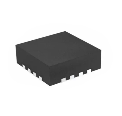
- 紧凑的封装:QFN3x3-16。
应用信息:
- 适用于机顶盒、网络PC、迷你笔记本电脑、接入点、路由器等。
封装信息:
- 封装类型:QFN3x3-16
- 封装标记:VJxyz(x=年份代码,y=周代码,z=批次号代码)