Boya Microelectronics
Memory Series
BY25Q80BS
8M BIT SPI NOR FLASH
Features
● Serial Peripheral Interface
- Standard SPI: SCLK, /CS, SI, SO, /WP, /HOLD
- Dual SPI: SCLK, /CS, IO0, IO1, /WP, /HOLD
- Quad SPI: SCLK, /CS, IO0, IO1, IO2, IO3
- QPI: SCLK, /CS, IO0, IO1, IO2, IO3
● Read
- Normal Read (Serial): 55MHz clock rate
- Fast Read (Serial): 108MHz clock rate with 30PF load
- Dual I/O data transfer up to 216Mbits/S
- Quad I/O data transfer up to 432Mbits/S
- Allows XIP (execute in place) Operation: Continuous Read with 8/16/32/64-byte Wrap
● Program
- Serial-input Page Program up to 256bytes
- Program Suspend and Resume
● Erase
- Block erase (64/32 KB)
- Sector erase (4 KB)
- Chip erase
- Erase Suspend and Resume
● Program/Erase Speed
- Page Program time: 0.6ms typical
- Sector Erase time: 50ms typical
- Block Erase time: 0.15/0.25s typical
- Chip Erase time: 4s typical
● Flexible Architecture
- Sector of 4K-byte
- Block of 32/64K-byte
● Low Power Consumption
- 20mA maximum active current
- 5uA maximum power down current
● Software/Hardware Write Protection
- 3x256-Byte Security Registers with OTP Locks
- Discoverable Parameters (SFDP) register
- Enable/Disable protection with WP Pin
- Write protect all/portion of memory via software
- Top or Bottom, Sector or Block selection
● Single Supply Voltage
- Full voltage range: 2.7~3.6V
● Temperature Range
- Commercial (0℃ to +70℃)
- Industrial (-40℃ to +85℃)
- Industrial (-40℃ to +105℃)
● Cycling Endurance/Data Retention
- Typical 100k Program-Erase cycles on any sector
- Typical 20-year data retention
Apr 2021
Rev 2.1
1 / 81
�Contents
BY25Q80BS
Contents
1. Description...................................................................................... 4
2. Signal Description .......................................................................... 6
2.1
2.2
2.3
2.4
2.5
2.6
2.7
2.8
2.9
Input/Output Summary.................................................................................. 6
Chip Select (/CS)........................................................................................... 6
Serial Clock (SCLK) ..................................................................................... 6
Serial Input (SI)/IO0...................................................................................... 6
Serial Data Output (SO)/IO1 ......................................................................... 7
Write Protect (/WP)/IO2 ............................................................................... 7
HOLD (/HOLD)/IO3..................................................................................... 7
VCC Power Supply ....................................................................................... 8
VSS Ground .................................................................................................. 8
3. Block/Sector Addresses ................................................................. 9
4. SPI Operation ............................................................................... 10
4.1
4.2
4.3
4.4
Standard SPI Instructions ............................................................................ 10
Dual SPI Instructions .................................................................................. 10
Quad SPI Instructions.................................................................................. 10
QPI Instructions........................................................................................... 10
5. Operation Features ...................................................................... 11
5.1
Supply Voltage .............................................................................................11
5.1.1 Operating Supply Voltage ............................................................... 11
5.1.2 Power-up Conditions ....................................................................... 11
5.1.3 Device Reset..................................................................................... 11
5.1.4 Power-down ...................................................................................... 11
5.2
Active Power and Standby Power Modes ....................................................11
5.3
Hold Condition .............................................................................................11
5.4
Status Register ............................................................................................. 13
5.4.1 Status Register Table ...................................................................... 13
5.4.2 The Status and Control Bits ........................................................... 13
5.4.3 Status Register Protect Table......................................................... 15
5.4.4 Write Protect Features .................................................................... 15
5.4.5 Status Register Memory Protection .............................................. 16
6. Device Identification ..................................................................... 17
7. Instructions Description................................................................ 18
7.1
Configuration and Status Instructions ......................................................... 23
7.1.1 Write Enable (06H) .......................................................................... 23
7.1.2 Write Disable (04H).......................................................................... 23
7.1.3 Read Status Register (05H or 35H) .............................................. 24
7.1.4 Write Status Register (01H or 31H) .............................................. 25
7.1.5 Write Enable for Volatile Status Register (50H) .......................... 27
7.1.6 Enter QPI Mode (38H)..................................................................... 28
7.1.7 Exit QPI Mode (FFH) ....................................................................... 28
7.2
Read Instructions ......................................................................................... 29
7.2.1 Read Data (03H) .............................................................................. 29
7.2.2 Fast Read (0BH) .............................................................................. 30
7.2.3 Dual Output Fast Read (3BH) ........................................................ 31
7.2.4 Quad Output Fast Read (6BH) ...................................................... 32
7.2.5 Dual I/O Fast Read (BBH) .............................................................. 33
7.2.6 Quad I/O Fast Read (EBH)............................................................. 35
7.2.7 Quad I/O Word Fast Read (E7H) .................................................. 37
Apr 2021
Rev 2.1
2 / 81
�Contents
BY25Q80BS
7.2.8 Octal Word Read Quad I/O (E3h).................................................. 39
7.2.9 Set Burst with Wrap (77H) .............................................................. 41
7.2.1 Set Read Parameters (C0H) .......................................................... 42
7.2.2 Burst Read with Wrap (0Ch) .......................................................... 42
7.3
ID and Security Instructions........................................................................ 44
7.3.1 Read Manufacture ID/ Device ID (90H)........................................ 44
7.3.2 Dual I/O Read Manufacture ID/ Device ID (92H) ........................ 45
7.3.3 Quad I/O Read Manufacture ID/ Device ID (94H) ...................... 46
7.3.4 Read JEDEC ID (9FH) .................................................................... 47
7.3.5 Read Unique ID Number (4Bh)...................................................... 48
7.3.6 Deep Power-Down (B9H) ............................................................... 49
7.3.7 Release from Deep Power-Down/Read Device ID (ABH)......... 50
7.3.8 Read Security Registers (48H) ...................................................... 52
7.3.9 Erase Security Registers (44H) ..................................................... 53
7.3.10 Program Security Registers (42H) ................................................ 54
7.3.11 Enable Reset (66H) and Reset Device (99H) ............................. 55
7.3.12 Read Serial Flash Discoverable Parameter (5AH) ..................... 56
7.4
Program and Erase Instructions................................................................... 57
7.4.1 Page Program (02H) ....................................................................... 57
7.4.2 Quad Page Program (32H)............................................................. 58
7.4.3 Fast Page Program (F2H) .............................................................. 59
7.4.4 Sector Erase (20H) .......................................................................... 60
7.4.5 32KB Block Erase (52H) ................................................................. 61
7.4.6 64KB Block Erase (D8H) ................................................................ 62
7.4.7 Chip Erase (60/C7H) ....................................................................... 63
7.4.8 Erase / Program Suspend (75H) ................................................... 64
7.4.9 Erase / Program Resume (7AH).................................................... 66
8. Electrical Characteristics.............................................................. 67
8.1
8.2
8.3
8.4
8.5
8.6
8.7
Absolute Maximum Ratings........................................................................ 67
Operating Ranges ........................................................................................ 67
Latch Up Characteristics ............................................................................. 68
Power-up Timing ......................................................................................... 68
DC Electrical Characteristics ...................................................................... 69
AC Measurement Conditions ...................................................................... 71
AC Electrical Characteristics ...................................................................... 71
9. Package Information .................................................................... 76
9.1
9.2
9.3
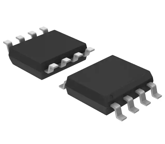
Package 8-Pin SOP 150- mil ........................................................................ 76
Package 8-Pin SOP 208- mil ........................................................................ 77
Package USON8 (2*3mm) .......................................................................... 78
10. Order Information ......................................................................... 79
10.1
10.2
Valid part Numbers and Top Side Marking ................................................. 80
Minimum Packing Quantity (MPQ)............................................................ 80
11. Document Change History........................................................... 81
Apr 2021
Rev 2.1
3 / 81
�Description
BY25Q80BS
1. Description
The BY25Q80BS is 8M-bit Serial Peripheral Interface(SPI) Flash memory, and supports the
Dual/Quad SPI as well as 2-clocks instruction cycle Quad Peripheral Interface (QPI): Serial Clock,
Chip Select, Serial Data I/O0 (SI), I/O1 (SO), I/O2 (/WP), and I/O3 (/HOLD) . The Dual I/O data is
transferred with speed of 216Mbits/s and the Quad I/O & Quad output data is transferred with speed
of 432Mbits/s. The device uses a single low voltage power supply, ranging from 2.7 Volt to 3.6 Volt.
Additionally, the device supports JEDEC standard manufacturer and device ID and three 256-bytes
Security Registers.
In order to meet environmental requirements, Boya Microelectronics offers 8-pin SOP 208mil, 8pad WSON 6x5-mm, and other special order packages, please contacts Boya Microelectronics for
ordering information.
Figure 1. Logic diagram
VCC
SCLK
SO
SI
/CS
BY25QXX
/WP
/HOLD
VSS
Figure 2. Pin Configuration SOP8
Top View
/CS
(IO1)SO
1
8
2
VCC
7
/HOLD(IO3)
SCLK
SOP8
Apr 2021
(IO2)/WP
3
6
VSS
4
5
Rev 2.1
SI(IO0)
4 / 81
�Description
BY25Q80BS
Figure 3.1. Pin Configuration WSON 5*6mm
/CS
1
8
VCC
(IO1)SO
2
7
/HOLD(IO3)
SCLK
Top View
(IO2)/WP
3
6
VSS
4
5
SI(IO0)
Figure 3.2. Pin Configuration USON 2*3mm
/CS
1
8
VCC
(IO1)SO
2
7
/HOLD(IO3)
Top View
Apr 2021
(IO2)/WP
3
6
SCLK
VSS
4
5
SI(IO0)
Rev 2.1
5 / 81
�Signal Description
BY25Q80BS
2. Signal Description
During all operations, VCC must be held stable and within the specified valid range: VCC (min) to
VCC (max).
All of the input and output signals must be held High or Low (according to voltages of VIH, VOH,
VIL or VOL, see Section 8.6, DC Electrical Characteristics on page 67&68). These signals are
described next.
2.1 Input/Output Summary
Table 1. Signal Names
Pin Name
I/O
/CS
I
SO (IO1)
I/O
/WP (IO2)
I/O
VSS
Chip Select
Serial Output for single bit data Instructions. IO1 for Dual or Quad
Instructions.
Write Protect in single bit or Dual data Instructions. IO2 in Quad mode.
The signal has an internal pull-up resistor and may be left unconnected
in the host system if not used for Quad Instructions.
Ground
SI (IO0)
I/O
SCLK
I
/HOLD (IO3)
I/O
VCC
Description
Serial Input for single bit data Instructions. IO0 for Dual or Quad
Instructions.
Serial Clock
Hold (pause) serial transfer in single bit or Dual data Instructions. IO3 in
Quad-I/O mode. The signal has an internal pull-up resistor and may be
left unconnected in the host system if not used for Quad Instructions.
Core and I/O Power Supply
2.2 Chip Select (/CS)
The chip select signal indicates when a instruction for the device is in process and the other signals
are relevant for the memory device. When the /CS signal is at the logic high state, the device is not
selected and all input signals are ignored and all output signals are high impedance. Unless an
internal Program, Erase or Write Status Registers embedded operation is in progress, the device
will be in the Standby Power mode. Driving the /CS input to logic low state enables the device,
placing it in the Active Power mode. After Power Up, a falling edge on /CS is required prior to the
start of any instruction.
2.3 Serial Clock (SCLK)
This input signal provides the synchronization reference for the SPI interface. Instructions,
addresses, or data input are latched on the rising edge of the SCLK signal. Data output changes
after the falling edge of SCLK.
2.4 Serial Input (SI)/IO0
This input signal is used to transfer data serially into the device. It receives instructions, addresses,
and data to be programmed. Values are latched on the rising edge of serial SCK clock signal.
SI becomes IO0 an input and output during Dual and Quad Instructions for receiving instructions,
addresses, and data to be programmed (values latched on rising edge of serial SCK clock signal)
as well as shifting out data (on the falling edge of SCK).
Apr 2021
Rev 2.1
6 / 81
�Signal Description
BY25Q80BS
2.5 Serial Data Output (SO)/IO1
This output signal is used to transfer data serially out of the device. Data is shifted out on the falling
edge of the serial SCK clock signal.
SO becomes IO1 an input and output during Dual and Quad Instructions for receiving instructions,
addresses, and data to be programmed (values latched on rising edge of serial SCK clock signal)
as well as shifting out data (on the falling edge of SCK).
2.6 Write Protect (/WP)/IO2
When /WP is driven Low (VIL), while the Status Register Protect bits (SRP1 and SRP0) of the
Status Registers (SR2[0] and SR1[7]) are set to 0 and 1 respectively, it is not possible to write to
the Status Registers. This prevents any alteration of the Status Registers. As a consequence, all
the data bytes in the memory area that are protected by the Block Protect, TB, SEC, and CMP bits
in the status registers, are also hardware protected against data modification while /WP remains
Low. The /WP function is not available when the Quad mode is enabled (QE) in Status Register 2
(SR2[1]=1).
The /WP function is replaced by IO2 for input and output during Quad mode for receiving addresses,
and data to be programmed (values are latched on rising edge of the SCK signal) as well as shifting
out data (on the falling edge of SCK). /WP has an internal pull-up resistance; when unconnected;
/WP is at VIH and may be left unconnected in the host system if not used for Quad mode.
2.7 HOLD (/HOLD)/IO3
The /HOLD function is only available when QE=0, If QE=1, The /HOLD function is disabled, the pin
acts as dedicated data I/O pin
The /HOLD signal goes low to stop any serial communications with the device, but doesn’t stop the
operation of write status register, programming, or erasing in progress.
The operation of HOLD, need /CS keep low, and starts on falling edge of the /HOLD signal, with
SCLK signal being low (if SCLK is not being low, HOLD operation will not start until SCLK being
low). The HOLD condition ends on rising edge of /HOLD signal with SCLK being low (If SCLK is
not being low, HOLD operation will not end until SCLK being low).
The Hold condition starts on the falling edge of the Hold (/HOLD) signal, provided that this coincides
with SCK being at the logic low state. If the falling edge does not coincide with the SCK signal being
at the logic low state, the Hold condition starts whenever the SCK signal reaches the logic low state.
Taking the /HOLD signal to the logic low state does not terminate any Write, Program or Erase
operation that is currently in progress.
/CS
SCLK
/HOLD
HOLD
HOLD
Apr 2021
Rev 2.1
7 / 81
�Signal Description
BY25Q80BS
2.8 VCC Power Supply
VCC is the supply voltage. It is the single voltage used for all device functions including read,
program, and erase.
2.9 VSS Ground
VSS is the reference for the VCC supply voltage.
Apr 2021
Rev 2.1
8 / 81
�Block/Sector Addresses
BY25Q80BS
3. Block/Sector Addresses
Table 2. Block/Sector Addresses of BY25Q80BS
Memory
Density
Block(64k
byte)
Block(32k
byte)
Sector 0
Sector
Size(KB)
4
000000h-000FFFh
:
:
:
Sector 7
4
007000h-007FFFh
Sector 8
4
008000h-008FFFh
:
4
:
Sector 15
4
00F000h-00FFFFh
Sector 16
4
010000h-010FFFh
:
:
:
Sector 23
4
017000h-017FFFh
Sector 24
4
018000h-018FFFh
:
:
:
Sector 31
4
01F000h-01FFFFh
:
:
:
Sector 224
4
0E0000h-0E0FFFh
Sector No.
Half block
0
Block 0
Half block
1
Half block
2
Block 1
Half block
3
8Mbit
:
:
Half block
28
Block 14
:
:
:
Sector 231
4
0E7000h-0E7FFFh
Sector 232
4
0E8000h-0E8FFFh
:
:
:
Sector 239
4
0EF000h-0EFFFFh
Sector 240
4
0F0000h-0F0FFFh
:
:
:
Sector 247
4
0F7000h-0F7FFFh
Sector 248
4
0F8000h-0F8FFFh
:
:
:
Sector 255
4
0FF000h-0FFFFFh
Half block
29
Half block
30
Block 15
Address range
Half block
31
Notes:
1. Block = Uniform Block, and the size is 64K bytes.
2. Half block = Half Uniform Block, and the size is 32k bytes.
3. Sector = Uniform Sector, and the size is 4K bytes.
Apr 2021
Rev 2.1
9 / 81
�SPI Operation
BY25Q80BS
4. SPI Operation
4.1 Standard SPI Instructions
The BY25Q80BS features a serial peripheral interface on 4 signals bus: Serial Clock (SCLK), Chip
Select (/CS), Serial Data Input (SI) and Serial Data Output (SO). Both SPI bus mode 0 and 3 are
supported. Input data is latched on the rising edge of SCLK and data shifts out on the falling edge
of SCLK.
4.2 Dual SPI Instructions
The BY25Q80BS supports Dual SPI operation when using the “Dual Output Fast Read” (3BH),
“Dual I/O Fast Read” (BBH) and “Read Manufacture ID/Device ID Dual I/O” (92H) instructions.
These instructions allow data to be transferred to or from the device at two times the rate of the
standard SPI. When using the Dual SPI instruction the SI and SO pins become bidirectional I/O
pins: IO0 and IO1.
4.3 Quad SPI Instructions
The BY25Q80BS supports Quad SPI operation when using the “Quad Output Fast Read”(6BH),
“Quad I/O Fast Read” (EBH) ,”Quad I/O word Fast Read”(E7H),”Read Manufacture ID/Device ID
Quad I/O”(94H) and “Quad Page Program”(32H) instructions. These instructions allow data to be
transferred to or from the device at four times the rate of the standard SPI. When using the Quad
SPI instruction the SI and SO pins become bidirectional I/O pins: IO0 and IO1, and /WP and /HOLD
pins become IO2 and IO3. Quad SPI instructions require the non -volatile Quad Enable bit (QE) in
Status Register to be set.
4.4 QPI Instructions
The BY25Q80BS supports Quad Peripheral Interface (QPI) operations only when the device is
switched from Standard/Dual/Quad SPI mode to QPI mode using the “Enter QPI (38h)” instruction.
The typical SPI protocol requires that the byte-long instruction code being shifted into the device
only via DI pin in eight serial clocks. The QPI mode utilizes all four IO pins to input the instruction
code, thus only two serial clocks are required. This can significantly reduce the SPI instruction
overhead and improve system performance in an XIP environment. Standard/Dual/Quad SPI mode
and QPI mode are exclusive. Only one mode can be active at any given time. “Enter QPI (38h)”
and “Exit QPI (FFh)” instructions are used to switch between these two modes. Upon power -up or
after a software reset using “Enable Reset (66h)”and “Reset (99h)” instruction, the default state of
the device is Standard/Dual/Quad SPI mode. To enable QPI mode, the non -volatile Quad Enable
bit (QE) in Status Register-2 is required to be set to 1. When using QPI instructions, the DI and DO
pins become bidirectional IO0 and IO1, and the /WP and /HOLD pins become IO2 and IO3
respectively.
Apr 2021
Rev 2.1
10 / 81
�Operation Features
BY25Q80BS
5. Operation Features
5.1 Supply Voltage
5.1.1
Operating Supply Voltage
Prior to selecting the memory and issuing instructions to it, a valid and stable VCC voltage within
the specified [VCC(min), VCC(max)] range must be applied (see operating ranges of page 65). In
order to secure a stable DC supply voltage, it is recommended to decouple the VCC line with a
suitable capacitor (usually of the order of 10nF to 100nF) close to the VCC/VSS package pins. This
voltage must remain stable and valid until the end of the transmission of the instruction and, for a
Write instruction, until the completion of the internal write cycle (tW).
5.1.2
Power-up Conditions
When the power supply is turned on, VCC rises continuously from VSS to VCC. During this time,
the Chip Select (/CS) line is not allowed to float but should follow the VCC voltage, it is therefore
recommended to connect the /CS line to VCC via a suitable pull-up resistor.
In addition, the Chip Select (/CS) input offers a built-in safety feature, as the /CS input is edge
sensitive as well as level sensitive: after power-up, the device does not become selected until a
falling edge has first been detected on Chip Select (/CS). This ensures that Chip Select (/CS) must
have been High, prior to going Low to start the first operation.
5.1.3
Device Reset
In order to prevent inadvertent Write operations during power -up (continuous rise of VCC), a power
on reset (POR) circuit is included. At Power-up, the device does not respond to any instruction until
VCC has reached the power on reset threshold voltage (this threshold is lower than the minimum
VCC operating voltage defined in Power-up Timing).
When VCC is lower than VWI , the device is reset.
5.1.4
Power-down
At Power-down (continuous decrease in VCC), as soon as VCC drops from the normal operating
voltage to below the power on reset threshold voltage, the device stops responding to any
instruction sent to it. During Power-down, the device must be deselected (Chip Select (/CS) should
be allowed to follow the voltage applied on VCC) and in Standby Power mode (that is there should
be no internal Write cycle in progress).
5.2 Active Power and Standby Power Modes
When Chip Select (/CS) is Low, the device is selected, and in the Active Power mode. The device
consumes ICC.
When Chip Select (/CS) is High, the device is deselected. If a Write cycle is not currently in progress,
the device then goes in to the Standby Power mode, and the device consumption drops to ICC1.
5.3 Hold Condition
The Hold (/HOLD) signal is used to pause any serial communications with the device without
resetting the clocking sequence. During the Hold condition, the Serial Data Output (SO) is high
impedance, and Serial Data Input (SI) and Serial Clock (SCLK) are Don’t Care. To enter the Hold
condition, the device must be selected, with Chip Select ( /CS) Low. Normally, the device is kept
selected, for the whole duration of the Hold condition. Deselecting the device while it is in the Hold
condition, has the effect of resetting the state of the device, and this mechanism can be used if it
is required to reset any processes that had been in progress.
Apr 2021
Rev 2.1
11 / 81
�Operation Features
BY25Q80BS
The Hold condition starts when the Hold (/HOLD) signal is driven Low at the same time as Serial
Clock (SCLK) already being Low (as shown in Figure 4).The Hold condition ends when the Hold
(HOLD) signal is driven High at the same time as Serial Clock (C) already being Low. Figure 4 also
shows what happens if the rising and falling edges are not timed to coincide with Serial Clock
(SCLK) being Low.
Figure 4. Hold condition activation
/CS
SCLK
/HOLD
HOLD
HOLD
Apr 2021
Rev 2.1
12 / 81
�Operation Features
BY25Q80BS
5.4 Status Register
5.4.1
Status Register Table
See Table 3 for detail description of the Status Register bits.
Table 3. Status Register
S15
SUS1
S14
CMP
S13
LB3
S12
LB2
S11
LB1
S10
SUS2
S9
QE
S8
SRP1
S7
S6
S5
S4
S3
S2
S1
S0
SRP0
BP4
BP3
BP2
BP1
BP0
WEL
WIP
5.4.2
The Status and Control Bits
5.4.2.1 WIP bit
The Write in Progress (WIP) bit indicates whether the memory is busy in program/erase/write status
register progress. When WIP bit sets to 1, means the device is busy in program/erase/write status
register progress, when WIP bit sets 0, means the device is not in program/erase/write status
register progress.
5.4.2.2 WEL bit
The Write Enable Latch bit indicates the status of the internal Write Enable Latch. When set to 1
the internal Write Enable Latch is set, when set to 0 the internal Write Enable Latch is reset and no
Write Status Register, Program or Erase instruction is accepted.
5.4.2.3 BP4, BP3, BP2, BP1, BP0 bits
The Block Protect (BP4, BP3, BP2, BP1, BP0) bits are non-volatile. They define the size of the
area to be software protected against Program and Erase instructions. These bits are written with
the Write Status Register instruction. When the Block Protect (BP4, BP3, BP2, BP1, BP0) bits are
set to 1, the relevant memory area (as defined in Table 6 and Table 7).becomes protected against
Page Program, Sector Erase and Block Erase instructions. The Block Protect ( BP4, BP3, BP2,
BP1, BP0) bits can be written provided that the Hardware Protected mod e has not been set. The
Chip Erase(CE) instruction is executed, if the Block Protect(BP2,BP1,BP0)bits are 0 and CMP=0
or The Block Protect (BP2, BP1, BP0) bits are1 and CMP=1.
5.4.2.4 SRP0, SRP1 bits
The Status Register Protect (SRP0 and SRP1) bits are non-volatile Read/Write bits in the status
register. The SRP bits control the method of write protection: software protection, hardware
protection, power supply lock-down or one time programmable protection.
5.4.2.5 QE bit
The Quad Enable (QE) bit is a non-volatile Read/Write bit in the Status Register that allows Quad
operation. When the QE bit is set to 0 (Default) the /WP pin and /HOLD pin are enable. When the
QE pin is set to 1, the Quad IO2 and IO3 pins are enabled. (Th e QE bit should never be set to 1
during standard SPI or Dual SPI operation if the /WP or /HOLD pins directly to the power supply or
ground).
Apr 2021
Rev 2.1
13 / 81
�Operation Features
BY25Q80BS
QE bit is required to be set to 1 before issuing an “Enter QPI (38h)” instruction to switch the device
from Standard/Dual/Quad SPI mode to QPI mode; otherwise the command (38h) will be ignored.
When the device is in QPI mode, QE bit will remain to be 1. A “Write Status Register” command in
QPI mode cannot change QE bit from 1 to 0.
5.4.2.6 LB bit
The LB bit is a non-volatile One Time Program (OTP) bit in Status Register (S13–S11) that provide
the write protect control and status to the Security Registers. The default state of LB is 0, the
security registers are unlocked. LB can be set to 1 individually using the Write Register instruction.
LB is One Time Programmable, once they are set to 1, the Security Registers will become read only permanently.
5.4.2.7 CMP bit
The CMP bit is a non-volatile Read/Write bit in the Status Register (S14). It is used in conjunction
the SEC-BP0 bits to provide more flexibility for the array protection. Please see the Status registers
Memory Protection table for details. The default setting is CMP=0.
5.4.2.8 SUS1/SUS2 bit
The SUS1 and SUS2 bits are read only bits in the status register2 (S15 and S10) that are set to
1 after executing an Erase/Program Suspend (75H) instruction (The Erase Suspend will set SUS1
to 1, and the Program Suspend will set the SUS2 to 1). The SUS1 and SUS2 bits are cleared to 0
by Erase/Program Resume (7AH) instruction as well as a power-down, power-up cycle.
Apr 2021
Rev 2.1
14 / 81
�Operation Features
5.4.3
BY25Q80BS
Status Register Protect Table
The Status Register Protect (SRP1 and SRP0) bits are non-volatile Read/Write bits in the Status
Register. The SRP bits control the method of write protection: software protection, hardware
protection, power supply lock-down or one time programmable protection.
Table 4. Status Register protect table
SRP1
SRP0
/WP
0
0
X
0
1
0
0
1
1
1
0
X
1
1
X
Status Register
Software
Protected
Hardware
Protected
Hardware
Unprotected
Description
The Status Register can be written to after a Write
Enable instruction, WEL=1.(Factory Default)
/WP=0, the Status Register locked and cannot be
written.
/WP=1, the Status Register is unlocked and can be
written to after a Write Enable instruction, WEL=1.
Power Supply
Lock-Down(1)
One Time
Program(2)
Status Register is protected and cannot be written to
again until the next Power-Down, Power-Up cycle.
Status Register is permanently protected and cannot
be written to.
Notes:
1. When SRP1, SRP0= (1, 0), a Power-Down, Power-Up cycle will change SRP1, SRP0 to
(0, 0) state.
2. The One time Program feature is available upon special order. Please contact Boya
Microelectronics for details.
5.4.4
1.
2.
3.
4.
5.
Write Protect Features
Software Protection: The Block Protect (BP4, BP3, BP2, BP1, BP0) bits define the section of
the memory array that can be read but not change.
Hardware Protection: /WP going low to protected the writable bits of Status Register.
Deep Power-Down: In Deep Power-Down Mode, all instructions are ignored except the
Release from deep Power-Down Mode instruction.
Write Enable: The Write Enable instruction is set the Write Enable Latch bit. The WEL bit will
return to reset by following situation:
-Power –up
-Write Disable
-Write Status Register (Whether the SR is protected, WEL will return to reset)
-Write Extended Address Register (when in 3-Byte Address Mode)
-Page Program (Whether the program area is protected, WEL will return to reset)
-Sector Erase/Block Erase/Chip Erase (Whether the erase area is protected, WEL will return
to reset)
-Software Reset
One Time Program (OTP) write protection for array and Security Registers using Status
Register.
Apr 2021
Rev 2.1
15 / 81
�Operation Features
5.4.5
BY25Q80BS
Status Register Memory Protection
5.4.5.1 Protect Table
Table 5. BY25Q80BS Status Register Memory Protection (CMP=0)
Status Register Content
BP4
X
0
0
0
0
0
0
0
0
0
X
1
1
1
1
1
1
1
1
BP3
X
0
0
0
0
1
1
1
1
X
X
0
0
0
0
1
1
1
1
BP2
0
0
0
0
1
0
0
0
1
1
1
0
0
0
1
0
0
0
1
BP1
0
0
1
1
0
0
1
1
0
0
1
0
1
1
0
0
1
1
0
BP0
0
1
0
1
0
1
0
1
0
1
X
1
0
1
X
1
0
1
X
Memory Content
Blocks
NONE
15
14 to 15
12 to 15
8 to 15
0
0 to 1
0 to 3
0 to 7
0 to 15
0 to 15
15
15
15
15
0
0
0
0
Addresses
NONE
0F0000H-0FFFFFH
0E0000H-0FFFFFH
0C0000H-0FFFFFH
080000H-0FFFFFH
000000H-00FFFFH
000000H-01FFFFH
000000H-03FFFFH
000000H-07FFFFH
000000H-0FFFFFH
000000H-0FFFFFH
0FF000H-0FFFFFH
0FE000H-0FFFFFH
0FC000H-0FFFFFH
0F8000H-0FFFFFH
000000H-000FFFH
000000H-001FFFH
000000H-003FFFH
000000H-007FFFH
Density
NONE
64KB
128KB
256KB
512KB
64KB
128KB
256KB
512KB
1MB
1MB
4KB
8KB
16KB
32KB
4KB
8KB
16KB
32KB
Portion
NONE
Upper 1/16
Upper 1/8
Upper 1/4
Upper 1/2
Lower 1/16
Lower 1/8
Lower 1/4
Lower 1/2
ALL
ALL
Top Block
Top Block
Top Block
Top Block
Bottom Block
Bottom Block
Bottom Block
Bottom Block
Table 6 BY25Q80BS Status Register Memory Protection (CMP=1)
Status Register Content
Memory Content
BP4
BP3
BP2
BP1
BP0
Blocks
Addresses
Density
Portion
X
0
0
0
0
0
0
0
0
0
0
1
1
1
1
X
0
0
0
0
1
1
1
1
X
X
0
0
0
0
0
0
0
0
1
0
0
0
1
1
1
0
0
0
1
0
0
1
1
0
0
1
1
0
0
1
0
1
1
0
0
1
0
1
0
1
0
1
0
1
X
1
0
1
X
0 to 15
0 to 14
0 to 13
0 to 11
0 to 7
1 to 15
2 to 15
4 to 15
8 to 15
NONE
NONE
0 to 15
0 to 15
0 to 15
0 to 15
000000H-0FFFFFH
000000H-0EFFFFH
000000H-0DFFFFH
000000H-0BFFFFH
000000H-07FFFFH
010000H-0FFFFFH
020000H-0FFFFFH
040000H-0FFFFFH
080000H-0FFFFFH
NONE
NONE
000000H-0FEFFFH
000000H-0FDFFFH
000000H-0FBFFFH
000000H-0F7FFFH
1MB
960KB
896KB
768KB
512KB
960KB
896KB
768KB
512KB
NONE
NONE
1020KB
1016KB
1008KB
992KB
ALL
Lower 15/16
Lower 7/8
Lower 3/4
Lower 1/2
Upper 15/16
Upper 7/8
Upper 3/4
Upper 1/2
NONE
NONE
L-255/256
L-127/128
L-63/64
L-31/32
1
1
1
1
1
1
1
1
0
0
0
1
0
1
1
0
1
0
1
X
0 to 15
0 to 15
0 to 15
0 to 15
001000H-0FFFFFH
002000H-0FFFFFH
004000H-0FFFFFH
008000H-0FFFFFH
1020KB
1016KB
1008KB
992KB
U-255/256
U-127/128
U-63/64
U-31/32
Apr 2021
Rev 2.1
16 / 81
�Device Identification
BY25Q80BS
6. Device Identification
Three legacy Instructions are supported to access device identification that can indicate the
manufacturer, device type, and capacity (density). The returned data bytes provide the information
as shown in the below table.
Table 7. BY25Q80BS ID Definition table
Operation Code
M7-M0
ID15-ID8
ID7-ID0
9FH
90H/92H/94H
68
68
40
14
13
ABH
Apr 2021
13
Rev 2.1
17 / 81
�Instructions Description
BY25Q80BS
7. Instructions Description
All instructions, addresses and data are shifted in and out of the device, beginning with the most
significant bit on the first rising edge of SCLK after /CS is driven low. Then, the one byte instruction
code must be shifted in to the device, most significant bit first on SI, each bit being latched on the
rising edges of SCLK.
See Table 8/9/10, every instruction sequence starts with a one-byte instruction code. Depending
on the instruction, this might be followed by address bytes, or by data bytes, or by both or none.
/CS must be driven high after the last bit of the instruction sequence has been shifted in. For the
instruction of Read, Fast Read, Read Status Register or Release from Deep Power Down, and
Read Device ID, the shifted-in instruction sequence is followed by a data out sequence. /CS can
be driven high after any bit of the data-out sequence is being shifted out.
For the instruction of Page Program, Sector Erase, Block Erase, Chip Erase, Write Status Register,
Write Enable, Write Disable or Deep Power-Down instruction, /CS must be driven high exactly at a
byte boundary, otherwise the instruction is rejected, and is not executed. That is /CS must driven
high when the number of clock pulses after /CS being driven low is an exact multiple of eight. For
Page Program, if at any time the input byte is not a full byte, nothing will happen and WEL will not
be reset.
Apr 2021
Rev 2.1
18 / 81
�Instructions Description
BY25Q80BS
Table 8. Instruction Set Table 1 (Standard/Dual/Quad SPI Instructions) (1)
Instruction Nam e
Byte 1
Write Enable
06h
Volatile SR Write Enable
50h
Write Disable
04h
Byte 2
05h
(S7-S0) (2)
01h
(S7-S0) (4)
Read Status Register-2
35h
(S15-S 8)(2)
Write Status Register-2
31h
(S15-S 8)
Chip Erase
C7h/60h
Erase Suspend
75h
Erase Resume
7Ah
Read Status Register-1
Write Status Register-1
(4)
Byte 3
Byte 4
Byte 5
Power-dow n
B9h
Release Power-dow n / ID
ABh
Dummy
Dummy
Dummy
(ID7-ID0)(2)
Manufactu rer/ D evic e ID
90h
Dummy
Dummy
00h
(MF7-MF0)
JEDEC ID
9Fh
(MF7-MF0)
(ID15-ID8)
(ID7-ID0)(2)
Enter QPI Mode
38h
Enable Reset
66h
Reset Device
Read Serial Flash
Discoverable
Paramet er
99h
5Ah
A23-A16
A15-A8
A7-A0
Dummy
Byte 6
(ID7-ID0)(2)
(D7-D0)
Next bytes
Instruction Nam e
Byte 1
Byte 2
Byte 3
Byte 4
Byte 5
Byte 6 ~ Byte 13
Read Unique ID
4Bh
Dummy
Dummy
Dummy
Dummy
(UID63-UID0)
Apr 2021
Rev 2.1
19 / 81
�Instructions Description
BY25Q80BS
Table 9. Instruction Set Table 2 (Standard/Dual/Quad SPI Instructions) (1)
Instruction Nam e
Byte 1
Byte 2
Byte 3
Page Program
02h
A23-A16
A15-A8
A7-A0
D7-D0(3)
Next bytes
Quad Page Program
32h
A23-A16
A15-A8
A7-A0
D7-D0(3)(9)
Next bytes
Sector Erase (4KB)
20h
A23-A16
A15-A8
A7-A0
Block Erase (32KB)
52h
A23-A16
A15-A8
A7-A0
Block Erase (64KB)
D8h
A23-A16
A15-A8
A7-A0
Read Data
03h
A23-A16
A15-A8
A7-A0
(D7-D0)
Fast Read
0Bh
A23-A16
A15-A8
A7-A0
Fast Read Dual Output
3Bh
A23-A16
A15-A8
A7-A0
Fast Read Quad Output
Erase Security Register
(5)
Program Security Register (5)
Read Security Register
(5)
Byte 4
6Bh
A23-A16
A15-A8
A7-A0
44h
A23-A16
A15-A8
A7-A0
42h
A23-A16
A15-A8
A7-A0
48h
A23-A16
A15-A8
A7-A0
(6)
(6)
Fast Read Dual I/O
BBh
A23-A16
Mftr./Device ID Dual I/O
92h
A23-A16(6) A15-A8(6)
A15-A8
A7-A0
Byte 5
Byte 6
Next bytes
Dummy
(D7-D0)
Next bytes
Dummy
(D7-D0)(7)
Next bytes
Dummy
(9)
Next bytes
Dummy
A7-A0(6)
(D7-D0)
M7-M0
(6)
(D7-D0)
(D7-D0)
M7-M0(6) (MF7-MF0)(7) (D7-D0)(7)
77h
Dummy
Dummy
Dummy
W8-W0
EBh
A23-A16(8)
A15-A8(8)
A7-A0(8)
M7-M0(8)
E7h
A23-A16
(8)
A15-A8
(8)
(8)
M7-M0
(8)
Dummy
A23-A16
(8)
A15-A8
(8)
M7-M0
(8)
(9)
A23-A16
(8)
A15-A8
(8)
M7-M0
(8)
Mftr./Device ID Quad I/O
Apr 2021
E3h
94h
A7-A0
(8)
A7-A0
(8)
A7-A0
Rev 2.1
Next bytes
(7)
Set Burst w ith Wrap
Word Read Quad I/O
Octal Word Read Quad
I/O(13)
Byte 9
Next bytes
Fast Read Quad I/O(10)
(11) (12)
Byte 8
(D7-D0)
D7-D0(3)
(6)
Byte 7
Dummy
(D7-D0)
Dummy
(D7-D0)(9)
Dummy
(D7-D0)
(9)
Next byte
Next bytes
Next bytes
Dummy
(MF7-MF0)(9) (ID7-ID0)(9)
20 / 81
�Instructions Description
BY25Q80BS
Table 10. Instruction Set Table 3 (QPI Instructions) (14)
Instruction Nam e
Byte 1
Write Enable
06h
Volatile SR Write Enable
50h
Write Disable
04h
Byte 2
Byte 3
05h
(S7-S0)(2)
Write Status Register-1
01h
(S7-S0)(4)
Read Status Register-2
35h
(S15-S8)(2)
Write Status Register-2
31h
(S15-S8)
Chip Erase
C7h/60h
Read Status Register-1
(4)
Erase Suspend
75h
Erase Resume
7Ah
Pow er-down
B9h
Set Read Parameters
C0h
P7-P0
Release Pow erdown / ID
ABh
Dummy
JEDEC ID
9Fh
Exit QPI Mode
FFh
Enable Reset
66h
(MF7-MF0 )
Byte 4
Dummy
(2)
(ID15-ID8)
Byte 5
Dummy
(2)
(ID7-ID0)
Byte 6
(ID7-ID0)(2)
(2)
Reset Device
99h
Page Program
02h
A23-A16
A15-A8
A7-A0
D7-D0(3)(9)
Next bytes
Sector Erase (4KB)
20h
A23-A16
A15-A8
A7-A0
Block Erase (32KB)
52h
A23-A16
A15-A8
A7-A0
Block Erase (64KB)
D8h
A23-A16
A15-A8
A7-A0
0Bh
A23-A16
A15-A8
A7-A0
Dummy (15)
(D7-D0)
0Ch
A23-A16
A15-A8
A7-A0
Dummy (15)
(D7-D0)
A7-A0
(15)
(D7-D0)
Fast Read
Burst Read w ith Wrap
(16)
Fast Read Quad I/O
EBh
A23-A16
A15-A8
M7-M0
Notes:
1. Data bytes are shifted with Most Significant Bit first. Byte fields with data in parenthesis
“( )” indicate data output from the device on 1, 2 or 4 IO pins.
2. The Status Register contents and Device ID will repeat continuously until /CS terminates
the instruction.
3. At least one byte of data input is required for Page Program, Quad Page Program and
Program Security Registers, up to 256 bytes of data input. If more than 256 bytes of
data are sent to the device, the addressing will wrap to the beginning of the page and
overwrite previously sent data.
4. Write Status Register-1 (01h) can also be used to program Status Register-1&2, see
section 7.1.4.
5. Security Register Address:
Security Register 1
A23-16 = 00h
A15-8 = 10h
A7-0 = byte address
Security Register 2
A23-16 = 00h
A15-8 = 20h
A7-0 = byte address
Security Register 3
A23-16 = 00h
A15-8 = 30h
A7-0 = byte address
6. Dual SPI address input format:
IO0 = A22, A20, A18, A16, A14, A12, A10, A8, A6, A4, A2, A0, M6, M4, M2, M0
IO1 = A23, A21, A19, A17, A15, A13, A11, A9, A7, A5, A3, A1, M7, M5, M3, M1
7. Dual SPI data output format:
IO0 = (D6, D4, D2, D0)
IO1 = (D7, D5, D3, D1)
8. Quad SPI address input format:
IO0 = A20, A16, A12, A8, A4, A0, M4, M0
IO1 = A21, A17, A13, A9, A5, A1, M5, M1
IO2 = A22, A18, A14, A10, A6, A2, M6, M2
IO3 = A23, A19, A15, A11, A7, A3, M7, M3
Apr 2021
Rev 2.1
21 / 81
�Instructions Description
BY25Q80BS
9. Quad SPI data input/output format:
IO0 = (D4, D0, …..)
IO1 = (D5, D1, …..)
IO2 = (D6, D2, …..)
IO3 = (D7, D3, …..)
10. Fast Read Quad I/O data output format:
IO0 = (x, x, x, x, D4, D0, D4, D0)
IO1 = (x, x, x, x, D5, D1, D5, D1)
IO2 = (x, x, x, x, D6, D2, D6, D2)
IO3 = (x, x, x, x, D7, D3, D7, D3)
11. Word Read Quad I/O data output format:
IO0 = (x, x, D4, D0, D4, D0, D4, D0)
IO1 = (x, x, D5, D1, D5, D1, D5, D1)
IO2 = (x, x, D6, D2, D6, D2, D6, D2)
IO3 = (x, x, D7, D3, D7, D3, D7, D3)
12. For Word Read Quad I/O, the lowest address bit must be 0. (A0 = 0)
13. For Octal Word Read Quad I/O, the lowest four address bits must be 0. (A3, A2, A1, A0 =
0)
14. QPI Command, Address, Data input/output format:
CLK # 0
1
2
3
4
5
6
7
8
9
10 11
IO0 = C4, C0,
A20, A16,
A12, A8,
A4, A0,
D4, D0,
D4, D0
IO1 = C5, C1,
A21, A17,
A13, A9,
A5, A1,
D5, D1,
D5, D1
IO2 = C6, C2,
A22, A18,
A14, A10,
A6, A2,
D6, D2,
D6, D2
IO3 = C7, C3,
A23, A19,
A15, A11,
A7, A3,
D7, D3,
D7, D3
15. The number of dummy clocks for QPI Fast Read, QPI Fast Read Quad I/O & QPI Burst
Read with Wrap is controlled by read parameter P7 – P4.
16. The wrap around length for QPI Burst Read with Wrap is controlled by read parameter P3
– P0.
Apr 2021
Rev 2.1
22 / 81
�Instructions Description
BY25Q80BS
7.1 Configuration and Status Instructions
7.1.1
Write Enable (06H)
See Figure 5, the Write Enable instruction is for setting the Write Enable Latch bit. The Write Enable
Latch bit must be set prior to every Page Program, Sector Erase, Block Erase, Chip Erase, Write
Status Register instruction and Erase/Program Security Registers instruction. The Write Enable
instruction sequence: /CS goes low sending the Write Enable instruction /CS goes high.
Figure 5. Write Enable Sequence Diagram for SPI Mode (left) or QPI Mode (right)
/CS
/CS
SCLK
Mode 3
Mode 3
Mode 0
0
1
2
3
4
5
6
7
Mode 3
Mode 0
06H
SO
High_Z
7.1.2
0
1
Mode 3
Mode 0
Mode 0
Instruction
06H
SI
(IO0)
SO
(IO1)
/WP
(IO2)
/HOLD
(IO3)
Instruction
SI
SCLK
Write Disable (04H)
See Figure 6, the Write Disable instruction is for resetting the Write Enable Latch bit. The Write
Disable instruction sequence: /CS goes low -> sending the Write Disable instruction -> /CS goes
high. The WEL bit is reset by following condition: Power-up and upon completion of the Write Status
Register, Page Program, Sector Erase, Block Erase and Chip Erase , Erase/Program Security
Registers and Reset instructions.
Figure 6. Write Disable Sequence Diagram for SPI Mode (left) or QPI Mode (right)
/CS
/CS
SCLK
Mode 3
Mode 3
Mode 0
0
1
2
3
4
5
6
04H
SO
High_Z
Apr 2021
Mode 3
Mode 0
SCLK
0
Rev 2.1
1
Mode 0
Mode 3
Mode 0
Instruction
04H
SI
(IO0)
SO
(IO1)
/WP
(IO2)
/HOLD
(IO3)
Instruction
SI
7
23 / 81
�Instructions Description
7.1.3
BY25Q80BS
Read Status Register (05H or 35H)
See Figure 7.a(SPI mode)& Figure 7.b (QPI mode)the Read Status Register (RDSR) instruction is
for reading the Status Register. The Status Register may be read at any time, even while a Program,
Erase or Write Status Register cycle is in progress. When one of these cycles is in progress, it is
recommended to check the Write in Progress (WIP) bit before sending a new instruction to the
device. It is also possible to read the Status Register continuously. For instruction code “05H”, the
SO will output Status Register bits S7~S0. The instruction code “35H”, the SO will output Status
Register bits S15~S8.
Figure 7.a. Read Status Register Sequence Diagram (SPI Mode)
/CS
SCLK
Mode 3
Mode 0
0
1
2
3
4
5
6
7
8
9
10
11
12
13
14
15
16
17
0
7
6
18
19
20
21
22
23
1
0
Instruction
SI
05H or 35H
SO
High_Z
Status Register-1/2 out
7
MSB
6
4
5
3
Status Register-1/2 out
1
2
5
4
3
MSB
Figure 7.b. Read Status Register Sequence Diagram (QPI Mode)
/CS
SCLK
Mode 3
Mode 0
0
1
2
3
4
5
Instruction
SI
(IO0)
Apr 2021
05H/35H
4
0
4
0
4
SO
(IO1)
5
1
5
1
5
/WP
(IO2)
6
2
6
2
6
/HOLD
(IO3)
7
3
7
3
7
SR-1/2
out
Rev 2.1
SR-1/2
out
24 / 81
2
7
�Instructions Description
7.1.4
BY25Q80BS
Write Status Register (01H or 31H)
See Figure 8.a (SPI mode)& Figure 8.b (QPI mode), the Write Status Register instruction allows
new values to be written to the Status Register. Before it can be accepted, a Write Enable
instruction must previously have been executed. After the Write Enable instruction has been
decoded and executed, the device sets the Write Enable Latch (WEL).
The Write Status Register instruction has no effect on S15, S1 and S0 of the Status Register. /CS
must be driven high after the eighth or sixteen bit of the data byte has been latched in. If not, the
Write Status Register instruction is not executed. As soon as /CS is driven high, the self -timed Write
Status Register cycle (whose duration is t W ) is initiated. While the Write Status Register cycle is in
progress, the Status Register may still be read to check the value of the Write in Progress (WIP)
bit. The Write in Progress (WIP) bit is 1 during the self-timed Write Status Register cycle, and is 0
when it is completed. When the cycle is completed, the Write Enable La tch is reset.
The Write Status Register instruction allows the user to change the values of the Block Protect
(BP4, BP3, BP2, BP1, BP0) bits, to define the size of the area that is to be treated as read -only, as
defined in Table 3. The Write Status Register instruction also allows the user to set or reset the
Status Register Protect (SRP1 and SRP0) bits in accordance with the Write Protect (/WP) signal.
The Status Register Protect (SRP1 and SRP0) bits and Write Protect (/WP) signal allow the device
to be put in the Hardware Protected Mode. The Write Status Register instruction is not executed
once the Hardware Protected Mode is entered.
Figure 8.a. Write Status Register Sequence Diagram (SPI mode)
/CS
0
1
2
3
4
5
6
7
8
9
10 11 12 13 14 15
SCLK
Status Register in
Instruction
SI
01H or 31H
7
6
5
2
3
4
1
0
MSB
High_Z
SO
Figure 8.b. Write Status Register Sequence Diagram (QPI mode)
/CS
SCLK
Mode 3
Mode 0
0
1
Instruction
SI
(IO0)
Apr 2021
01H/31H
2
3
SR1/2in
4
0
SO
(IO1)
5
1
/WP
(IO2)
6
2
/HOLD
(IO3)
7
3
Rev 2.1
Mode 3
Mode 0
25 / 81
�Instructions Description
BY25Q80BS
The BY25Q80BS is also backward compatible to BoyaMicro’s previous generations of serial flash
memories, in which the Status Register-1&2 can be written using a single “Write Status Register-1
(01h)” command. To complete the Write Status Register- 1&2 instruction, the /CS pin must be driven
high after the sixteenth bit of data that is clocked in as shown in Figure 8.c(SPI mode) & Figure
8.d(QPI mode). If /CS is driven high after the eighth clock, the Write Status Register -1 (01h)
instruction will only program the Status Register-1, the Status Register-2 will not be affected
(Previous generations will clear CMP and QE bits).
Figure 8.c. Write Status Register-1/2 Instruction (SPI Mode)
/CS
SCLK
Mode 3
Mode 0
0
1
2
3
4
5
6
7
8
9
11
12
13
14
15
1
0
16
17
01H
6
7
MSB
5
4
2
3
18
19
20
21
22
23
9
8
Status Register-2 in
Status Register-1 in
Instruction
SI
10
15
14
13
12
11
10
MSB
SO
High_Z
Figure 8.d. Write Status Register-1/2 Instruction (QPI Mode)
/CS
SCLK
Mode 3
Mode 0
0
1
Instruction
SI
(IO0)
Apr 2021
01H
2
3
SR1 in
4
5
SR2 in
4
0
12
8
SO
(IO1)
5
1
13
9
/WP
(IO2)
6
2
14
10
/HOLD
(IO3)
7
3
15
11
Rev 2.1
Mode 3
Mode 0
26 / 81
Mode 3
Mode 0
�Instructions Description
7.1.5
BY25Q80BS
Write Enable for Volatile Status Register (50H)
See Figure 9, the non-volatile Status Register bits can also be written to as volatile bits. This gives
more flexibility to change the system configuration and memory protection schemes quickly without
waiting for the typical non-volatile bit write cycles or affecting the endurance of the Status Register
non-volatile bits. Write Enable for Volatile Status Register instruction will not set the Write Enable
Latch bit, it is only valid for the Write Status Registers instruction to change the volatile Status
Register bit values.
Figure 9. Write Enable for Volatile Status Register Instruction for SPI Mode (left) or QPI Mode (right)
/CS
/CS
SCLK
Mode 3
Mode 3
Mode 0
0
1
2
3
4
5
6
50H
SO
High_Z
Apr 2021
Mode 3
Mode 0
SCLK
0
Rev 2.1
1
Mode 0
Mode 3
Mode 0
Instruction
50H
SI
(IO0)
SO
(IO1)
/WP
(IO2)
/HOLD
(IO3)
Instruction
SI
7
27 / 81
�Instructions Description
7.1.6
BY25Q80BS
Enter QPI Mode (38H)
The BY25Q80BS support both Standard/Dual/Quad Serial Peripheral Interface (SPI) and Quad
Peripheral Interface (QPI). However, SPI mode and QPI mode cannot be used at the same time.
“Enter QPI (38h)” instruction is the only way to switch the device from SPI mode to QPI mode.
Upon power-up, the default state of the device upon is Standard/Dual/Quad SPI mode. This
provides full backward compatibility with earlier generations of BoyaMicro serial flash memories.
See Instruction Set Table 1- 2 for all supported SPI commands. In order to switch the device to QPI
mode, the Quad Enable (QE) bit in Status Register-2 must be set to 1 first, and an “Enter QPI (38h)”
instruction must be issued. If the Quad Enable (QE) bit is 0, the “Enter QPI (38h)” i nstruction will
be ignored and the device will remain in SPI mode.
See Instruction Set Table 3 for all the commands supported in QPI mode.
When the device is switched from SPI mode to QPI mode, the existing Write Enable and Eras e
Suspend status, and the Wrap Length setting will remain unchanged.
Figure 42. Enter QPI Instruction (SPI Mode only)
/CS
SCLK
0
Mode 3
Mode 0
1
2
3
4
5
6
7
Mode 3
Mode 0
Instruction
7.1.7
SI
38H
SO
High_Z
Exit QPI Mode (FFH)
In order to exit the QPI mode and return to the Standard/Dual/Quad SPI mode, an “Exit QPI (FFh)”
instruction must be issued.
When the device is switched from QPI mode to SPI mode, the existing Write Enable Latch (WEL)
and Erase Suspend status, and the Wrap Length setting will remain unchanged.
Figure 43. Exit QPI Instruction (QPI Mode only)
/CS
Mode 3
SCLK
0
1
Mode 0
Mode 3
Mode 0
Instruction
FFH
SI
(IO0)
SO
(IO1)
/WP
(IO2)
/HOLD
(IO3)
Apr 2021
Rev 2.1
28 / 81
�Instructions Description
BY25Q80BS
7.2 Read Instructions
7.2.1
Read Data (03H)
See Figure 10, the Read Data Bytes (READ) instruction is followed by a 3-byte address (A23-A0),
each bit being latched-in during the rising edge of SCLK. Then the memory content, at that address,
is shifted out on SO, each bit being shifted out, at a Max frequency fR, during the falling edge of
SCLK. The address is automatically incremented to the next higher address after each byte of data
is shifted out allowing for a continuous stream of data. This means that the entire memory can be
accessed with a single command as long as the clock continues. The command is completed by
driving /CS high. The whole memory can be read with a single Read Data Bytes (READ) instruction.
Any Read Data Bytes (READ) instruction, while an Erase, Program or Write cycle is in progress, is
rejected without having any effects on the cycle that is in progress.
The Read Data (03h) instruction is only supported in Standard SPI mode.
Figure 10. Read Data Bytes Sequence Diagram (SPI Mode only)
/CS
0
1
2
3
4
5
6
7
8
9
10
28 29 30
31 32 33 34 35 36 37 38 39
SCLK
24-Bit Address
Instruction
SI
03H
23 22
21
3
2
1
0
Data Byte1
MSB
High_Z
SO
Apr 2021
7
MSB
Rev 2.1
6
5
4
3
High_Z
2
29 / 81
1
0
�Instructions Description
7.2.2
BY25Q80BS
Fast Read (0BH)
See Figure 11.a, the Read Data Bytes at Higher Speed (Fast Read) instruction is for quickly reading
data out. It is followed by a 3-byte address (A23-A0) and a dummy byte, each bit being latched-in
during the rising edge of SCLK. Then the memory content, at that address, is s hifted out on SO,
each bit being shifted out, at a Max frequency fc, during the falling edge of SCLK. The first byte
addressed can be at any location. The address is automatically incremented to the next higher
address after each byte of data is shifted out.
Figure 11.a. Fast Read Sequence Diagram (SPI Mode)
/CS
0
1
2
4
3
5
6
7
9
8
28
10
29
30
31
SCLK
Instruction
24-Bit Address
0BH
SI
23
22
21
41
42
43
3
2
46
47
1
0
High_Z
SO
/CS
32
33
34
35
36
37 38
39
40
44
45
SCLK
Dummy Clocks
High_Z
SI
Data byte 1
High_Z
SO
6
7
5
4
High_Z
3
2
0
1
Fast Read (0Bh) in QPI Mode
The Fast Read instruction is also supported in QPI mode. When QPI mode is enabled, the number
of dummy clocks is configured by the “Set Read Parameters (C0h)” instruction to accommodate a
wide range of applications with different needs for either maximum Fast Read frequency or
minimum data access latency. Depending on the Read Parameter Bits P[5:4] setting, the number
of dummy clocks can be configured as either 4, 4, 6 or 8. The default number of dummy clocks
upon power up or after a Reset instruction is 4.
Figure 11.b. Fast Read Instruction (QPI Mode)
/CS
SCLK
Mode 3
Mode 0
0
1
2
3
4
5
6
Instruction
SI
(IO0)
0Bh
A23-16
7
8
A7-0
A15-8
9
10
11
12
13
14
15
IOs switch from
Input to Output
Dummy*
20
16
12
8
4
0
4
0
4
0
4
0
4
0
4
SO
(IO1)
21
17
13
9
5
1
5
1
5
1
5
1
5
1
5
/WP
(IO2)
22
18
14
10
6
2
6
2
6
2
6
2
6
2
6
/HOLD
(IO3)
23
19
15
11
7
3
7
3
7
3
7
3
7
3
7
Byte 1
Byte 2
*”Set Read Parameters” instruction(C0h)can
set the number of dummy clocks.
Apr 2021
Rev 2.1
30 / 81
�Instructions Description
7.2.3
BY25Q80BS
Dual Output Fast Read (3BH)
See Figure 12, the Dual Output Fast Read instruction is followed by 3-byte address (A23-A0) and
a dummy byte, each bit being latched in during the rising edge of SCLK, then the memory contents
are shifted out 2-bit per clock cycle from SI and SO. The first byte addressed can be at any location.
The address is automatically incremented to the next higher address after each byte of data is
shifted out.
Figure 12. Dual Output Fast Read Sequence Diagram (SPI Mode only)
/CS
0
1
2
3
4
5
6
7
9
8
28
10
29
30
31
SCLK
Instruction
24-Bit Address
3BH
SI
SO
23
22
21
41
42
43
3
2
1
0
High_Z
/CS
32
33
34
35
36
37
38
39
40
44
45
46
47
6
4
2
0
SCLK
Dummy Clocks
SI
6
4
2
0
Data Byte 2
Data Byte 1
High_Z
SO
Apr 2021
7
Rev 2.1
5
3
1
7
5
3
1
31 / 81
High_Z
High_Z
�Instructions Description
7.2.4
BY25Q80BS
Quad Output Fast Read (6BH)
See Figure 13, the Quad Output Fast Read instruction is followed by 3-byte address (A23-A0) and
a dummy byte, each bit being latched in during the rising edge of SCLK, then the memory contents
are shifted out 4-bit per clock cycle from IO3, IO2, IO1 and IO0. The first byte addressed can be at
any location. The address is automatically incremented to the next higher address after each byte
of data is shifted out.
Figure 13. Quad Output Fast Read Sequence Diagram (SPI Mode only)
/CS
0
1
3
2
4
5
6
8
7
9
28
10
29
30
31
SCLK
24-Bit Address
Instruction
SI
(IO0)
6BH
SO
(IO1)
High_Z
/WP
(IO2)
High_Z
/HOLD
(IO3)
High_Z
/CS
32
33
34
35
36
22
23
37
38
39
40
3
2
1
45
46
47
21
41
42
4
0
4
0
4
0
4
0
5
1
5
1
5
1
5
1
6
2
6
2
6
2
6
2
7
3
Byte1
7
3
7
3
Byte3
43
44
0
SCLK
SI
(IO0)
Dummy Clocks
SO
(IO1)
High_Z
/WP
(IO2)
High_Z
/HOLD
(IO3)
High_Z
Apr 2021
Rev 2.1
Byte2
3
7
Byte4
High_Z
High_Z
High_Z
High_Z
32 / 81
�Instructions Description
7.2.5
BY25Q80BS
Dual I/O Fast Read (BBH)
See Figure 14.a, the Dual I/O Fast Read instruction is similar to the Dual Output Fast Read
instruction but with the capability to input the 3-byte address (A23-0) and a “Continuous Read Mode”
byte 2-bit per clock by SI and SO, each bit being latched in during the rising edge of SCLK, then
the memory contents are shifted out 2-bit per clock cycle from SI and SO. The first byte addressed
can be at any location. The address is automatically incremented to the next higher address after
each byte of data is shifted out.
Dual I/O Fast Read with “continuous Read Mode”
The Dual I/O Fast Read instruction can further reduce instruction overhead through setting the
“continuous Read Mode” bits (M7-4) after the inputs 3-byte address A23-A0).If the “continuous
Read Mode” bits(M5-4)=(1,0),then the next Dual I/O fast Read instruction (after CS/ is raised and
then lowered) does not require the BBH instruction code. The instruction sequence is shown in the
following Figure14.b.If the “continuous Read Mode” bits (M5-4) does not equal (1,0),the next
instruction requires the first BBH instruction code, thus returning to normal operation. A “continuous
Read Mode” Reset instruction can be used to reset (M5-4) before issuing normal instruction.
Figure 14.a. Dual I/O Fast Read Sequence Diagram (Initial command or previous (M5-4) ≠
(1,0)),SPI mode only)
/CS
0
1
2
3
4
5
6
7
9
8
10 11 12
13 14 15 16 17 18 19 20 21 22 23
SCLK
Instruction
SI
(IO0)
BBH
SO
(IO1)
High_Z
6
4
2
0
6
4
2
0
6
4
2
0
6
4
2
0
7
5
3
1
7
5
3
1
7
5
3
1
7
5
3
1
A23-16
A15-8
A7-0
M7-0
/CS
SCLK
23 24 25 26
27 28 29 30
31 32 33
34 35 36 37 38 39
SI
(IO0)
6
4
2
0
6
4
2
0
6
4
2
0
6
4
2
0
SO
(IO1)
7
5
3
1
7
5
3
1
7
5
3
1
7
3
5
Byte 4
1
Byte 1
Apr 2021
Byte 2
Byte 3
Rev 2.1
High_Z
High_Z
33 / 81
�Instructions Description
BY25Q80BS
Figure 14.b. Dual I/O Fast Read Sequence Diagram (Previous command set (M5 -4) =(1,0),SPI
mode only)
/CS
0
1
2
3
4
5
6
7
8
9 10 11 12 13 14 15
SCLK
SI
(IO0)
6
SO
(IO1)
7
/CS
Apr 2021
0
6
4
0
6
4
2
0
6
4
2
0
5 3 1
A23-16
7
5 3 1
A15-8
7
5 3
A7-0
1
7
5 3
M7-0
1
4
2
2
15 16 17 18 19 20 21 22 23 24 25 26 27 28 29 30 31
SCLK
SI
(IO0)
6
4
2
0
6
4
0
6
4
2
0
6
SO
(IO1)
7
5 3
Byte1
1
7
5 3 1
Byte2
7
5 3
Byte3
1
7
2
Rev 2.1
2
0
5 3
Byte4
1
4
34 / 81
�Instructions Description
7.2.6
BY25Q80BS
Quad I/O Fast Read (EBH)
See Figure 15.a, the Quad I/O Fast Read instruction is similar to the Dual I/O Fast Read instruction
but with the capability to input the 3-byte address (A23-0) and a “Continuous Read Mode” byte and
4-dummy clock 4-bit per clock by IO0, IO1, IO3, IO4, each bit being latched in during the rising
edge of SCLK, then the memory contents are shifted out 4-bit per clock cycle from IO0, IO1, IO2,
IO3. The first byte addressed can be at any location. The address is automatically incremented to
the next higher address after each byte of data is shifted out. The Quad Enable bit (QE) of Status
Register must be set to enable for the Quad I/O Fast read instruction.
Quad I/O Fast Read with “Continuous Read Mode”
The Quad I/O Fast Read instruction can further reduce instruction overhead through setting the
“Continuous Read Mode” bits (M7-0) after the input Address bits (A23-0), as shown in Figure 16, If
the “Continuous Read Mode” bits (M5-4 )= (1,0), then the next Fast Read Quad I/O instruction(after
/CS is raised and then lowered) does not require the EBH instruction code, The instruction
sequence is shown in the followed Figure 15.b . If the “Continuous Read Mode” bits M5-4 do not
equal to (1,0), the next instruction requires the first EBH instruction code, thus returning to normal
operation. A “Continuous Read Mode” Reset command can also be used to reset (M5 -4) before
issuing normal command.
Figure 15.a. Quad I/O Fast Read Sequence Diagram (Initial command or previous (M5-4≠
(1,0)),SPI mode)
/CS
SCLK
Mode 3
Mode 0
0
1
2
3
4
5
6
7
9
A23-16
Instruction
SI
(IO0)
8
10
11
12
A15-8
13
A7-0
14
15
M7-0
16
17
Dummy
18
19
20
22
21
23
IOs switch from
Input to Output
Dummy
20
16
12
8
4
0
4
0
4
0
4
0
4
SO
(IO1)
21
17
13
9
5
1
5
1
5
1
5
1
5
/WP
(IO2)
22
18
14
10
6
2
6
2
6
2
6
2
6
/HOLD
(IO3)
23
19
15
11
7
3
7
3
7
3
7
3
7
EBH
Byte1
Byte2
Byte3
Figure 15.b. Quad I/O Fast Read Sequence Diagram (Previous command set (M5 -4)=(1,0)), SPI
mode)
/CS
SCLK
Mode 3
Mode 0
0
1
A23-16
2
3
4
A15-8
5
A7-0
6
7
M7-0
8
9
Dummy
10
11
12
13
14
15
IOs switch from
Input to Output
Dummy
SI
(IO0)
20
16
12
8
4
0
4
0
4
0
4
0
4
SO
(IO1)
21
17
13
9
5
1
5
1
5
1
5
1
5
/WP
(IO2)
22
18
14
10
6
2
6
2
6
2
6
2
6
/HOLD
(IO3)
23
19
15
11
7
3
7
3
7
3
7
3
Byte1
Byte2
7
Byte3
Quad I/O Fast Read with “8/16/32/64-Byte Wrap Around”
The Quad I/O Fast Read instruction can also be used to access a specific portion within a page by
issuing a “Set Burst with Wrap” (77H) instruction prior to EBH. The “Set Burst with Wrap” (77H)
instruction can either enable or disable the “Wrap Around” feature for the following EBH instructions.
When “Wrap Around” is enabled, the data being accessed can be limited to either an 8, 16, 32 or
64-byte section of a 256-byte page. The output data starts at the initial address specified in the
instruction, once it reaches the ending boundary of the 8/16/32/64 -byte section, the output will wrap
around to the beginning boundary automatically until /CS is pulled high to terminate the instruction.
Apr 2021
Rev 2.1
35 / 81
�Instructions Description
BY25Q80BS
The Burst with Wrap feature allows applications that use cache to quickly fetch a critical address
and then fill the cache afterwards within a fixed length (8/16/32/64 -byte) of data without issuing
multiple read instructions.
The “Set Burst with Wrap” instruction allows three “Wrap Bits”, W6-4 to be set. The W4 bit is used
to enable or disable the “Wrap Around” operation while W6-5 are used to specify the length of the
wrap around section within a page.
Quad I/O Fast Read (EBh) in QPI Mode
The Quad I/O Fast Read instruction is also supported in QPI mode, as shown in Figure 15.c Figure 15.d. When QPI mode is enabled, the number of dummy clocks is configured by the “Set
Read Parameters (C0h)” instruction to accommodate a wide range of applications with different
needs for either maximum Fast Read frequency or minimum data access latency. Depen ding on
the Read Parameter Bits P[5:4] setting, the number of dummy clocks can be configured as either
4, 4, 6 or 8. The default number of dummy clocks upon power up or after a Reset instruction is 4.
In QPI mode, the “Continuous Read Mode” bits M7-0 are also considered as dummy clocks. In the
default setting, the data output will follow the Continuous Read Mode bits immediately.
“Continuous Read Mode” feature is also available in QPI mode for Quad I/O Fast Read instruction.
Please refer to the description on previous pages.
“Wrap Around” feature is not available in QPI mode for Quad I/O Fast Read instruction. To perform
a read operation with fixed data length wrap around in QPI mode, a dedicated “Burst Read with
Wrap” (0Ch) instruction must be used.
Figure 15.c. Quad I/O Fast Read Sequence Diagram (Initial instruction or previous (M5 -4≠(1,0)) ,
QPI mode)
/CS
SCLK
0
Mode 3
Mode 0
1
2
3
4
5
6
Instruction
A23-16
EBH
SI
(IO0)
7
A7-0
A15-8
8
9
10
11
12
13
14
IOs switch from
Input to Output
M7-0*
20
16
12
8
4
0
4
0
4
0
4
0
4
SO
(IO1)
21
17
13
9
5
1
5
1
5
1
5
1
5
/WP
(IO2)
22
18
14
10
6
2
6
2
6
2
6
2
6
/HOLD
(IO3)
23
19
15
11
7
3
7
3
7
3
7
3
Byte 1
Byte 2
7
Byte 3
*”Set Read Parameters” instruction(C0h)can
set the number of dummy clocks.
Figure 15.d. Quad I/O Fast Read Sequence Diagram (Initial instruction or previous (M5 -4=(1,0)) ,
QPI mode)
/CS
0
SCLK
SI
(IO0)
SO
(IO1)
/WP
(IO2)
/HOLD
(IO3)
2
1
3
6
5
4
7
8
9
10 11
4
0
4
0
4
0
4
0
4
0
4
0
5
1
5
1
5
1
5
1
5
1
5
1
6
2
6
2
6
2
6
2
6
2
6
2
7
3
7
3
7
3
7
3
7 3
Byte1
A23-16
A15-8
A7-0
M7-0*
7 3
Byte2
*”Set Read Parameters” instruction(C0h)can set
the number of dummy clocks.
Apr 2021
Rev 2.1
36 / 81
�Instructions Description
7.2.7
BY25Q80BS
Quad I/O Word Fast Read (E7H)
The Quad I/O Word Fast Read instruction is similar to the Quad Fast Read instruction except that
the lowest address bit (A0) must equal 0 and 2-dummy clock. The instruction sequence is shown
in the followed Figure 16.a, the first byte addressed can be at any location. The address is
automatically incremented to the next higher address after each byte of data is shifted out. The
Quad Enable bit (QE) of Status Register (S9) must be set to enable for the Quad I/O Word Fast
Read instruction.
Quad I/O Word Fast Read with “Continuous Read Mode”
The Quad I/O Word Fast Read instruction can further reduce instruction overhead through setting
the “Continuous Read Mode” bits (M7-0) after the input 3-byte Address bits (A23-0). If the
“Continuous Read Mode” bits (M5-4) = (1, 0), then the next Quad I/O Fast Read instruction (after
/CS is raised and then lowered) does not require the E7H instruction code, the instruction sequence
is shown in the followed Figure 16.b. If the “Continuous Read Mode” bits M5-4 do not equal to
(1,0), the next instruction requires the first E7H instruction code, thus returning to normal operation.
A “Continuous Read Mode” Reset command can also be used to reset (M5-4) before issuing normal
command.
Figure 16.a. Quad I/O Word Fast Read Sequence Diagram (Initial command or previous (M5-4)≠
(1,0),SPI mode only)
/CS
0
1
2
3
4
5
6
9 10 11 12 13 14 15 16 17 18 19 20 21 22 23
8
7
SCLK
SI
(IO0)
Instruction
E7H
SO
(IO1)
High_Z
/WP
(IO2)
High_Z
/HOLD
(IO3)
High_Z
4
0
4
0
4
0
4
0
4
0
4
0
4
0
5
1
5
1
5
1
5
1
5
1
5
1
5
1
6
2
6
2
6
2
6
2
6
2
6
2
6
2
7 3 7 3
A23-16 A15-8
7 3
A7-0
7 3
M7-M0 Dummy
7
3
Byte1
7 3
Byte2
7 3
Byte3
Figure 16.b. Quad I/O word Fast Read Sequence Diagram (Previous command set (M5 -4) =(1,0),
SPI mode only)
/CS
0
SCLK
SI
(IO0)
SO
(IO1)
/WP
(IO2)
/HOLD
(IO3)
1
3
4
6
5
7
8
9 10 11 12 13 14 15
4
0
4
0
4
0 4
0
4
0
4
0
4
0
5
1
5
1
5
1
5
1
5
1
5
1
5
1
6
2
6
2
6
2
6
2
6
2
6
2
6
2
7
3
7
3
7
3
7
A23-16
Apr 2021
2
A15-8
A7-0
7 3
Dummy Byte1
M7-0
Rev 2.1
3
7 3
Byte2
7 3
Byte3
37 / 81
�Instructions Description
BY25Q80BS
Quad I/O Word Fast Read with “8/16/32/64-Byte Wrap Around” in standard SPI mode
The Quad I/O Fast Read instruction can also be used to access a specific portion within a page by
issuing a “Set Burst with Wrap” (77H) instruction prior to E7H. The “Set Burst with Wrap” (77H)
instruction can either enable or disable the “Wrap Around” feature for the following E7H instructions.
When “Wrap Around” is enabled, the data being accessed can be limited to either an 8, 16, 32 or
64-byte section of a 256-byte page. The output data starts at the initial address specified in the
instruction, once it reaches the ending boundary of the 8/16/32/64-byte section, the output will wrap
around to the beginning boundary automatically until /CS is pulled high to terminate the instruction.
The Burst with Wrap feature allows applications that use cache to quickly fetch a critical address
and then fill the cache afterwards within a fixed length (8/16/32/64 -byte) of data without issuing
multiple read instructions.
The “Set Burst with Wrap” instruction allows three “Wrap Bits”, W6-4 to be set. The W4 bit is used
to enable or disable the “Wrap Around” operation while W6-5 are used to specify the length of the
wrap around section within a page.
Apr 2021
Rev 2.1
38 / 81
�Instructions Description
7.2.8
BY25Q80BS
Octal Word Read Quad I/O (E3h)
The Octal Word Read Quad I/O (E3h) instruction is similar to the Fast Read Quad I/O (EBh)
instruction except that the lower four Address bits (A0, A1, A2, A3) must equal 0. As a result, the
dummy clocks are not required, which further reduces the instruction overhead allowing even faster
random access for code execution (XIP). The Quad Enable bit (QE) of Status Register-2 must be
set to enable the Octal Word Read Quad I/O Instruction.
Octal Word Read Quad I/O with “Continuous Read Mode”
The Octal Word Read Quad I/O instruction can further reduce instruction overhead thro ugh setting
the “Continuous Read Mode” bits (M7- 0) after the input Address bits (A23-0), as shown in Figure
17.a. The upper nibble of the (M7-4) controls the length of the next Octal Word Read Quad I/O
instruction through the inclusion or exclusion of the first byte instruction code. The lower nibble bits
of the (M3-0) are don’t care (“x”). However, the IO pins should be high-impedance prior to the falling
edge of the first data out clock.
If the “Continuous Read Mode” bits M5-4 = (1,0), then the next Octal Word Read Quad I/O
instruction (after /CS is raised and then lowered) does not require the E3h instruction code, as
shown in Figure 17.b. This reduces the instruction sequence by eight clocks and allows the Read
address to be immediately entered after /CS is asserted low. If the “Continuous Read Mode” bits
M5-4 do not equal to (1,0), the next instruction (after /CS is raised and then lowered) requires the
first byte instruction code, thus returning to normal operation. It is recommended to input FFh on
SI for the next instruction (8 clocks), to ensure M4 = 1 and return the device to normal operation.
Figure 17.a. Octal Word Read Quad I/O Instruction (Initial instruction or previous M5 -4 ≠ 10, SPI
Mode only)
/CS
SCLK
Mode 3
Mode 0
0
1
2
3
4
Instruction
SI
(IO0)
5
6
7
8
9
A23-16
10
11
12
A15-8
13
A7-0
14
15
16
17
18
19
20
21
IOs switch from
Input to Output
M7-0
20
16
12
8
4
0
4
0
4
0
4
0
4
0
4
SO
(IO1)
21
17
13
9
5
1
5
1
5
1
5
1
5
1
5
/WP
(IO2)
22
18
14
10
6
2
6
2
6
2
6
2
6
2
6
/HOLD
IO3
23
19
15
11
7
3
7
3
7
3
7
3
7
3
E3H
Byte1
Byte2
Byte3
7
Byte4
Figure 17.b. Octal Word Read Quad I/O Instruction (Previous instruction set M5-4 = 10, SPI Mode
only)
Apr 2021
Rev 2.1
39 / 81
�Instructions Description
BY25Q80BS
/CS
SCLK
Mode 3
Mode 0
0
1
A23-16
2
3
4
A15-8
5
A7-0
6
7
8
9
10
11
12
13
IOs switch from
Input to Output
M7-0
SI
(IO0)
20
16
12
8
4
0
4
0
4
0
4
0
4
0
4
SO
(IO1)
21
17
13
9
5
1
5
1
5
1
5
1
5
1
5
/WP
(IO2)
22
18
14
10
6
2
6
2
6
2
6
2
6
2
6
/HOLD
(IO3)
23
19
15
11
7
3
7
3
7
3
7
3
7
3
7
Byte1
Apr 2021
Rev 2.1
Byte2
Byte3
40 / 81
Byte4
�Instructions Description
7.2.9
BY25Q80BS
Set Burst with Wrap (77H)
See Figure 18, The Set Burst with Wrap instruction is used in conjunction with ”Quad I/O Fast Read”
and “Quad I/O Word Fast Read” instruction to access a fixed length of 8/16/32/64-byte section
within a 256-byte page, in standard SPI mode.
The Set Burst with Wrap instruction sequence:/CS goes low ->Send Set Burst with Wrap instruction
->Send24 Dummy bits ->Send 8 bits “Wrap bits”->/CS goes high.
If W6-4 is set by a Set Burst with Wrap instruction, all the following “Fast Read Quad I/O” and “Word
Read Quad I/O” instructions will use the W6-4 setting to access the 8/16/32/64-byte section within
any page. To exit the “Wrap Around” function and return to normal read operation, another Set
Burst with Wrap instruction should be issued to set W4=1. The default value of W4 upon power on
is 1.
W4 = 0
W4 =1 (DEFAULT)
W6 , W5
Wrap Around
Wrap Length
Wrap Around
Wrap Length
0
0
Yes
8-byte
No
N/A
0
1
Yes
16-byte
No
N/A
1
0
Yes
32-byte
No
N/A
1
1
Yes
64-byte
No
N/A
Figure 18. Set Burst with Wrap Sequence Diagram (SPI mode only)
/CS
0
1
2
3
4
5
6
7
8
9
11
10
12
13
14
15
SCLK
SI
(IO0)
SO
(IO1)
Instruction
x
x
x
x
x
x
W4
x
High_Z
x
x
x
x
x
x
x
High_Z
W5
x
x
x
x
x
x
x
High_Z
W6
x
x
x
x
x
x
x
x
High_Z
/WP
(IO2)
High_Z
/HOLD
(IO3)
High_Z
Byte1
Apr 2021
High_Z
77H
Rev 2.1
Byte2
Byte3
Byte4
41 / 81
�Instructions Description
BY25Q80BS
7.2.1 Set Read Parameters (C0H)
In QPI mode, to accommodate a wide range of applications with different needs for either maximum
read frequency or minimum data access latency, “Set Read Parameters (C0h)” instruction can be
used to configure the number of dummy clocks for “Fast Read (0Bh)”, “Fast Read Quad I/O (EBh)”
& “Burst Read with Wrap (0Ch)” instructions, and to configure the number of bytes of “Wrap Length”
for the “Burst Read with Wrap (0Ch)” instruction.
In Standard SPI mode, the “Set Read Parameters (C0h)” instruction is not accepted. The dummy
clocks for various Fast Read instructions in Standard/Dual/Quad SPI mode are fixed, please refer
to the Instruction Table 2 for details. The “Wrap Length” is set by W5-4 bit in the “Set Burst with
Wrap (77h)” instruction. This setting will remain unchanged when the device is switched from
Standard SPI mode to QPI mode.
The default “Wrap Length” after a power up or a Reset instruction is 8 bytes, the default numbe r of
dummy clocks is 4. The number of dummy clocks is only programmable for “Fast Read (0Bh)”,
“Fast Read Quad I/O (EBh)” & “Burst Read with Wrap (0Ch)” instructions in the QPI mode.
Whenever the device is switched from SPI mode to QPI mode, the number of dummy clocks and
“Wrap Length” should be set again, prior to any 0Bh, EBh or 0Ch instructions.
P5 – P4
DUMMY
CLOCKS
MAXIMUM
READ
FREQ.
MAXIMUM
READ FREQ.
(A[1:0]=0,0
VCC=2.7V~2.9V)
MAXIMUM
READ
FREQ.
(A[1:0]=0,0
VCC=3.0V~3.6V)
P1 – P0
WRAP
LENGTH
0
0
4
55MHz
80MHz
80MHz
0
0
8-byte
0
1
4
55MHz
80MHz
80MHz
0
1
16-byte
1
0
6
80MHz
80MHz
108MHz
1
0
32-byte
1
1
8
80MHz
80MHz
108MHz
1
1
64-byte
Figure 41. Set Read Parameters Instruction (QPI Mode only)
/CS
SCLK
Mode 3
Mode 0
0
1
Instruction
SI
(IO0)
7.2.2
C0H
2
3
Mode 3
Mode 0
Read
Parameters
P4
P0
SO
(IO1)
P5
P1
/WP
(IO2)
P6
P2
/HOLD
(IO3)
P7
P3
Burst Read with Wrap (0Ch)
The “Burst Read with Wrap (0Ch)” instruction provides an alternative way to perform the read
operation with “Wrap Around” in QPI mode. The instruction is similar to the “ Fast Read (0Bh)”
instruction in QPI mode, except the addressing of the read operation will “Wrap Around” to the
beginning boundary of the “Wrap Length” once the ending boundary is reached.
The “Wrap Length” and the number of dummy clocks can be configured by the “ Set Read
Parameters (C0h)” instruction.
Apr 2021
Rev 2.1
42 / 81
�Instructions Description
BY25Q80BS
Figure 19. Burst Read with Wrap Instruction (QPI Mode only)
/CS
Mode 3
SCLK
0
1
2
3
4
5
6
7
8
9
10
11
12
13
14
15
Mode 0
Instruction
A23-16
0CH
SI
(IO0)
A15-8
A7-0
IOs switch from
Input to Output
Dummy*
20
16
12
8
4
0
4
0
4
0
4
SO
(IO1)
21
17
13
9
5
1
5
1
5
1
5
/WP
(IO2)
22
18
14
10
6
2
6
2
6
2
6
/HOLD
(IO3)
23
19
15
11
7
3
7
3
7
3
7
Byte1
Byte2
*”Set Read Paraments” instruction(C0h)can
set the number of dummy clocks.
Apr 2021
Rev 2.1
43 / 81
Byte3
�Instructions Description
BY25Q80BS
7.3 ID and Security Instructions
7.3.1
Read Manufacture ID/ Device ID (90H)
See Figure 20, The Read Manufacturer/Device ID instruction is an alternative to the Release from
Power-Down/Device ID instruction that provides both the JEDEC assigned Manufacturer ID and
the specific Device ID.
The instruction is initiated by driving the /CS pin low and shifting the instruction code “90H” followed
by a 24-bit address (A23-A0) of 000000H. If the 24-bit address is initially set to 000001H, the Device
ID will be read first.
Figure 20. Read Manufacture ID/ Device ID Sequence Diagram (SPI Mode only)
/CS
0
1
2
3
4
5
6
7
8
9
10
28 29 30 31
SCLK
Instruction
SI
24-Bit Address
3 2
23 22 21
90H
High_Z
SO
1
0
/CS
32 33 34 35 36
37 38 39 40 41 42
43 44 45 46 47
SCLK
SI
SO
Apr 2021
7
6
Manufacturer ID
5 4
3 2
1
0
7
Rev 2.1
6
5
Device ID
3 2
4
1
0
44 / 81
�Instructions Description
7.3.2
BY25Q80BS
Dual I/O Read Manufacture ID/ Device ID (92H)
See Figure 21, the Dual I/O Read Manufacturer/Device ID instruction is an alternative to the
Release from Power-Down/Device ID instruction that provides both the JEDEC assigned
Manufacturer ID and the specific Device ID by Dual I/O.
The instruction is initiated by driving the /CS pin low and shifting the instruction code “92H” followed
by a 24-bit address (A23-A0) of 000000H. If the 24-bit address is initially set to 000001H, the Device
ID will be read first.
Figure 21. Dual I/O Read Manufacture ID/ Device ID Sequence Diagram (SPI Mode only)
/CS
0
1
2
4
3
5
6
7
9
8
10 11 12
13 14 15 16 17 18 19 20 21 22 23
SCLK
Instruction
SI
(IO0)
92H
SO
(IO1)
High_Z
6
4
2
0
6
4
2
0
6
4
2
0
6
4
2
0
7
5
3
1
7
5
3
1
7
5
3
1
7
5
3
1
A23-16
A15-8
A7-0
Dummy
/CS
SCLK
23 24 25 26
27 28 29 30
SI
(IO0)
6
4
2
0
6
4
2
0
SO
(IO1)
7
5
3
1
7
5
3
1
40 41 42 43
6
44 45 46 47
0
6
7
5 3 1
MFR ID(repeat)
7
4
2
4
2
0
High_Z
High_Z
MFR ID
Apr 2021
39
31 32
Device ID
MFR and Device ID
(repeat)
Rev 2.1
3 1
5
Device ID(repeat)
45 / 81
�Instructions Description
7.3.3
BY25Q80BS
Quad I/O Read Manufacture ID/ Device ID (94H)
See Figure 22, the Quad I/O Read Manufacturer/Device ID instruction is an alternative to the
Release from Power-Down/Device ID instruction that provides both the JEDEC assigned
Manufacturer ID and the specific Device ID by quad I/O.
The instruction is initiated by driving the /CS pin low and shifting the instruction code “94H” followed
by a 24-bit address (A23-A0) of 000000H and4 dummy clocks. If the 24-bit address is initially set
to 000001H, the Device ID will be read first.
Figure 22. Quad I/O Read Manufacture ID/ Device ID Sequence Diagram (SPI mode only)
/CS
0
1
2
3
4
5
6
7
9
8
10 11 12
13 14 15 16 17 18 19 20 21
22 23
SCLK
Instruction
SI
(IO0)
94H
SO
(IO1)
High_Z
WP
(IO2)
High_Z
HOLD
(IO3)
High_Z
4
0
4
0
4
0
4
0
4
0
4
0
5
1
5
1
5
1
5
1
5
1
5
1
6
2
6
2
6
2
6
2
6
2
6
2
7
3
7
3
7
3
7
3
7
3
7
3
A23-16
A15-8
A7-0
dummy
dummy
MFR ID Device ID
/CS
SCLK
23 24 25 26
27 28 29 30
31
SI
(IO0)
4
0
4
0
4
0
4
0
SO
(IO1)
5
1
5
1
5
1
5
1
WP
(IO2)
6
2
6
2
6
2
6
2
7
3
7
3
7
3
7
3
HOLD
(IO3)
Apr 2021
MFR ID DID ID MFR ID DID ID
(repeat) (repeat) (repeat) (repeat)
Rev 2.1
46 / 81
�Instructions Description
7.3.4
BY25Q80BS
Read JEDEC ID (9FH)
The JEDEC ID instruction allows the 8-bit manufacturer identification to be read, followed by two
bytes of device identification. The device identification indicates the memory type in the first byte,
and the memory capacity of the device in the second byte. JEDEC ID instruction while an Erase or
Program cycle is in progress, is not decoded, and has no effect on the cycle that is in progress.
The JEDEC ID instruction should not be issued while the device is in Deep Power -Down Mode.
See Figure 23.a (SPI mode)&Figure 23.b (QPI mode), The device is first selected by driving /CS to
low. Then, the 8-bit instruction code for the instruction is shifted in. This is followed by the 24-bit
device identification, stored in the memory, being shifted out on Serial Data Output, each bit being
shifted out during the falling edge of Serial Clock. The JEDEC ID instruction is terminat ed by driving
/CS to high at any time during data output. When /CS is driven high, the device is put in the Standby
Mode. Once in the Standby Mode, the device waits to be selected, so that it can receive, decode
and execute instructions.
Figure 23.a. JEDEC ID Sequence Diagram (SPI Mode)
/CS
0
1
2
3
6
5
4
7
8
10
9
11 12 13
14 15
SCLK
9FH
Instruction
SI
Manufacturer ID
/CS
6
7
MSB
SO
16 17 18 19
20 21 22 23 24
5
25 26
3
4
27 28 29
2
0
1
30 31
SCLK
SI
SO
7
Memory Type ID15-ID8
1
6 5 4 3 2
0
MSB
6
7
Capacity ID7-ID0
5 4 3 2 1
0
MSB
Figure 23.b. Read JEDEC ID Instruction (QPI Mode)
/CS
SCLK
Mode 3
Mode 0
0
1
2
Instruction
SI
(IO0)
4
5
6
7
Mode 3
Mode 0
IOs switch from
Input to Output
9FH
12
8
4
0
SO
(IO1)
13
9
5
1
/WP
(IO2)
14
10
6
2
15
11
7
3
/HOLD
(IO3)
68H
Apr 2021
3
Rev 2.1
ID15-8
ID7-0
47 / 81
�Instructions Description
7.3.5
BY25Q80BS
Read Unique ID Number (4Bh)
The Read Unique ID Number instruction accesses a factory-set read-only 64-bit number that is
unique to each BY25Q80BS device. The ID number can be used in conjunction with user software
methods to help prevent copying or cloning of a system. The Read Unique ID instruction is initiated
by driving the /CS pin low and shifting the instruction code “4Bh” followed by a four b ytes of dummy
clocks. After which, the 64-bit ID is shifted out on the falling edge of SCLK as shown in Figure 24.
Figure 24. Read Unique ID Sequence Diagram (SPI Mode only)
/CS
SCLK
0
Mode 3
Mode 0
1
2
3
4
5
6
7
8
9
10
Instruction
SI
11
12
13
14
15
16
Dummy Byte 1
17
18
19
20
21
22
23
Dummy Byte 2
4BH
SO
High_Z
/CS
23
24
25
26
27
28
29
30
31
32
33
34
35
36
37
38
39
40
41
100 101 102 103
SCLK
Dummy Byte 3
Dummy Byte 4
SI
SO
Apr 2021
High_Z
63
MSB
Rev 2.1
62
2
1
0
64-bit Unique
Serial Number
48 / 81
Mode 3
Mode 0
�Instructions Description
7.3.6
BY25Q80BS
Deep Power-Down (B9H)
Although the standby current during normal operation is relatively low, standby current can be
further reduced with the Deep Power-down instruction. The lower power consumption makes the
Deep Power-down (DPD) instruction especially useful for battery powered applications (see ICC1
and ICC2). The instruction is initiated by driving the /CS pin low and shifting the instruction code
“B9h” as shown in Figure 25.a (SPI mode) &Figure 25.b (QPI mode).
The /CS pin must be driven high after the eighth bit has been latched. If this is not done the Deep
Power down instruction will not be executed. After /CS is driven high, the power -down state will
entered within the time duration of tDP. While in the power -down state only the Release from Deep
Power-down / Device ID instruction, which restores the device to normal operation, will be
recognized. All other Instructions are ignored. This includes the Read Status Register instruction,
which is always available during normal operation. Ignoring all but one instruction also makes the
Power Down state a useful condition for securing maximum write protection. The device always
powers-up in the normal operation with the standby current of ICC1.
Figure 25.a. Deep Power-Down Sequence Diagram (SPI mode)
/CS
0
1
2
3 4
5
6
tDP
7
SCLK
Instruction
SI
B9H
Stand-by mode
Power-down mode
Figure 25.b. Deep Power-down Instruction (QPI Mode)
/CS
tDP
Mode 3
SCLK
0
1
Mode 3
Mode 0
Mode 0
Instruction
B9H
SI
(IO0)
SO
(IO1)
/WP
(IO2)
/HOLD
(IO3)
Stand-by current
Apr 2021
Rev 2.1
Power-down current
49 / 81
�Instructions Description
7.3.7
BY25Q80BS
Release from Deep Power-Down/Read Device ID (ABH)
The Release from Power-Down or Device ID instruction is a multi-purpose instruction. It can be
used to release the device from the Power-Down state or obtain the devices electronic identification
(ID) number.
See Figure 26.a (SPI mode) &Figure 26.b (QPI mode), to release the device from the Power-Down
state, the instruction is issued by driving the /CS pin low, shifting the instruction code “ABH” and
driving /CS high Release from Power-Down will take the time duration of tRES1 (See AC
Characteristics) before the device will resume normal operation and other instruction are accepted.
The /CS pin must remain high during the tRES1 time duration.
When used only to obtain the Device ID while not in the Power -Down state, the instruction is
initiated by driving the /CS pin low and shifting the instruction code “ABH” followed by 3 -dummy
byte. The Device ID bits are then shifted out on the falling edge of SCLK with most significant bit
(MSB) first as shown in The Device ID value for the BY25Q80BS is listed in Manufacturer and
Device Identification table. The Device ID can be read continuously. The instruction is completed
by driving /CS high.
When used to release the device from the Power-Down state and obtain the Device ID, the
instruction is the same as previously described, and shown in Figure 26.c (SPI mode) &Figure 26.d
(QPI mode), except that after /CS is driven high it must remain high for a time duration of tRES2
(See AC Characteristics). After this time duration the device will resume normal operation and other
instruction will be accepted. If the Release from Power-Down/Device ID instruction is issued while
an Erase, Program or Write cycle is in process (when WIP equal 1) the instruction is ignored and
will not have any effects on the current cycle.
Figure 26.a. Release Power-Down Sequence Diagram (SPI mode)
/CS
0
1
2
3
4
5
6
tRES1
7
SCLK
Instruction
SI
ABH
Power-down mode
Stand-by mode
Figure 26.b. Release Power-down Instruction (QPI Mode)
/CS
tRES1
Mode 3
SCLK
0
1
Mode 3
Mode 0
Mode 0
Instruction
ABH
SI
(IO0)
SO
(IO1)
/WP
(IO2)
/HOLD
(IO3)
Power-down current Stand-by current
Apr 2021
Rev 2.1
50 / 81
�Instructions Description
BY25Q80BS
Figure 26.c. Release Power-down / Device ID Instruction (SPI Mode)
/CS
SCLK
Mode 3
Mode 0
0
1
2
3
4
5
6
7
8
9
23
22
Instruction
SI
29
30
31
1
0
32
33
34
35
36
37
38
Mode 3
Mode 0
39
tRES2
3 Dummy Bytes
ABH
2
MSB
High_Z
SO
Device ID
5
6
7
MSB
4
3
2
1
0
Power-down current Stand-by current
Figure 26.d. Release Power-down / Device ID Instruction (QPI Mode)
/CS
tRES2
Mode 3
SCLK
0
1
2
3
5
6
7
9
8
Mode 3
Mode 0
Mode 0
Instruction
IOs switch from
Input to Output
3 Dummy Byte
ABH
SI
(IO0)
SO
(IO1)
/WP
(IO2)
/HOLD
(IO3)
4
X
X
X
X
X
X
4
0
X
X
X
X
X
X
5
1
X
X
X
X
X
X
6
2
X
X
X
X
X
X
7
3
Device ID
Power-down current Stand-by current
Apr 2021
Rev 2.1
51 / 81
�Instructions Description
7.3.8
BY25Q80BS
Read Security Registers (48H)
See Figure 27, the Read Security Registers instruction is similar to Fast Read instruction. The
instruction is followed by a 3-byte address (A23-A0) and a dummy byte, each bit being latched-in
during the rising edge of SCLK. Then the memory content, at that address, is s hifted out on SO,
each bit being shifted out, at a Max frequency fC, during the falling edge of SCLK. The first byte
addressed can be at any location. The address is automatically incremented to the next higher
address after each byte of data is shifted out. Once the A7-A0 address reaches the last byte of the
register (Byte FFH), it will reset to 000H, the instruction is completed by driving /CS high.
Address
A23-A16
A15-A12
A11-A8
A7-A0
Security Registers 1
00H
0001
0000
Byte Address
Security Registers 2
00H
0010
0000
Byte Address
Security Registers 3
00H
0011
0000
Byte Address
Figure 27. Read Security Registers instruction Sequence Diagram (SPI Mode only)
/CS
0
1
2
3
4
5
6
7
8
9
28 29 30 31
SCLK
Instruction
SI
48H
SO
High_Z
24-Bit Address
3
23 22
2
1
0
/CS
32 33 34 35 36 37 38 39 40 41 42 43 44 45 46 47
SCLK
Dummy Byte
SI
SO
Apr 2021
7
6
5
4
3
2
1
0
Data Byte 1
7 6
MSB
Rev 2.1
5
4
3
2
1
0
52 / 81
�Instructions Description
7.3.9
BY25Q80BS
Erase Security Registers (44H)
The BY25Q80BS provides three 256-byte Security Registers which can be erased and
programmed individually. These registers may be used by the system manufacturers to store
security and other important information separately from the main memory array.
See Figure 28, the Erase Security Registers instruction is similar to Sector/Block Erase instruction.
A Write Enable instruction must previously have been executed to set the Write Enable Latch bit.
The Erase Security Registers instruction sequence: /CS goes low sending Erase Security Registers
instruction /CS goes high. /CS must be driven high after the eighth bit of the instruction code has
been latched in otherwise the Erase Security Registers instruction is not executed. As soon as /CS
is driven high, the self-timed Erase Security Registers cycle (whose duration is tSE) is initiated.
While the Erase Security Registers cycle is in progress, the Status Register may be read to check
the value of the Write In Progress (WIP) bit. The Write In Progress (WIP) bit is 1 during the selftimed Erase Security Registers cycle, and is 0 when it is completed. At some unspecified time
before the cycle is completed, the Write Enable Latch bit is reset. The Security Registers Lock Bit
(LB) in the Status Register can be used to OTP protect the security registers. Once the LB bit is
set to 1, the Security Registers will be permanently locked; the Erase Security Registers instruction
will be ignored.
Address
A23-A16
A15-A12
A11-A8
A7-A0
Security Registers 1
00H
0001
0000
Byte Address
Security Registers 2
00H
0010
0000
Byte Address
Security Registers 3
00H
0011
0000
Byte Address
Figure 28. Erase Security Registers instruction Sequence Diagram (SPI Mode only)
/CS
0
1
2
3
4
5
6
7
8
9
29 30 31
SCLK
Instruction
SI
Apr 2021
44H
Rev 2.1
24-Bit Address
23 22
2
1
0
53 / 81
�Instructions Description
BY25Q80BS
7.3.10 Program Security Registers (42H)
See Figure 29, the Program Security Registers instruction is similar to the Page Program instruction.
It allows from 1 to 256 bytes Security Registers data to be programmed. A Write Enable instruction
must previously have been executed to set the Write Enable Latch bit before sending the Program
Security Registers instruction. The Program Security Registers instruction is entered by driving /CS
Low, followed by the instruction code (42H), 3-byte address and at least one data byte on SI. As
soon as /CS is driven high, the self-timed Program Security Registers cycle (whose duration is tPP)
is initiated. While the Program Security Registers cycle is in progress, the Status Register may be
read to check the value of the Write In Progress (WIP) bit. The Write In Progress (WIP) bit is 1
during the self-timed Program Security Registers cycle, and is 0 when it is completed. At some
unspecified time before the cycle is completed, the Write Enable Latch bit is rese t.
If the Security Registers Lock Bit (LB3/LB2/LB1) is set to 1, the Security Registers will be
permanently locked. Program Security Registers instruction will be ignored.
Address
A23-A16
A15-A12
A11-A8
A7-A0
Security Registers 1
00H
0001
0000
Byte Address
Security Registers 2
00H
0010
0000
Byte Address
Security Registers 3
00H
0011
0000
Byte Address
Figure 29. Program Security Registers instruction Sequence Diagram (SPI Mode only)
/CS
0
4
3
2
1
5
6
7
9
8
10
29 30
28
31 32 33 34 35 36 37 38 39
SCLK
Instruction
24-Bit Address
23 22
MSB
42H
SI
21
3
Data Byte 1
1
2
0
7
MSB
6
4
5
2
3
1
0
2079
2078
2077
2076
2075
2074
53 54 55
2073
40 41 42 43 44 45 46 47 48 49 50 51 52
2072
/CS
SCLK
Data Byte 2
SI
7
MSB
Apr 2021
6
5
4
3
2
1
0
7 6
MSB
Data Byte 3
4 3 2
5
Rev 2.1
1
0
7 6
MSB
Data Byte 256
3 2
5 4
54 / 81
1
0
�Instructions Description
BY25Q80BS
7.3.11 Enable Reset (66H) and Reset Device (99H)
Because of the small package and the limitation on the number of pins, the BY25Q 80BS provides
a software Reset instruction instead of a dedicated RESET pin. Once the software Reset instruction
is accepted, any on-going internal operations will be terminated and the device will return to its
default power-on state and lose all the current volatile settings, such as Volatile Status Register
bits, Write Enable Latch (WEL) status, Program/Erase Suspend status, Continuous Read Mode bit
setting (M7-M0) and Wrap Bit setting (W6-W4).
To avoid accidental reset, both “Enable Reset (66h)” and “Reset (99h)” instructions must be issued
in sequence. Any other commands other than “Reset (99h)” after the “Enable Reset (66h)”
command will disable the “Reset Enable” state. A new sequence of “Enable Reset (66h)” and
“Reset (99h)” is needed to reset the device. Once the Reset command is accepted by the device,
the device will take approximately 30us to reset. During this period, no command will be accepted.
The Enable Reset (66h) and Reset (99h) instruction sequence is shown in Figure 30.a(SPI mode)&
Figure 30.b(QPI mode) .
Data corruption may happen if there is an on-going or suspended internal Erase or Program
operation when Reset command sequence is accepted by the device. It is recommended to check
the BUSY bit and the SUS bit in Status Register before issuing the Reset comman d sequence.
Figure 30.a. Enable Reset (66h) and Reset (99h) Command Sequence (SPI mode)
/CS
0
1
2
3
4
5
6
0
7
1
2
3
4
5
6
SCLK
Instruction
SI
Instruction
99h
66H
Figure 30.b. Enable Reset and Reset Instruction Sequence (QPI Mode)
/CS
SCLK
SI
(IO0)
Mode 3
Mode 0
0
1
Mode 3
Mode 0
0
1
Instruction
Instruction
66H
99H
Mode 3
Mode 0
SO
(IO1)
/WP
(IO2)
/HOLD
(IO3)
Apr 2021
Rev 2.1
55 / 81
7
�Instructions Description
BY25Q80BS
7.3.12 Read Serial Flash Discoverable Parameter (5AH)
See Figure 31,The Serial Flash Discoverable Parameter (SFDP) standard provides a consistent
method of describing the functional and feature capabilities of serial flash devices in a standard
set of internal parameter tables. These parameter tables can be interrogated by host system
software to enable adjustments needed to accommodate divergent features from multiple
vendors. The concept is similar to the one found in the Introduction of JEDEC Standar d, JESD68
on CFI. SFDP is a standard of JEDEC Standard No.216.
Figure 31. Read Serial Flash Discoverable Parameter command Sequence Diagram
/CS
0
1
2
3
4
5
6
7
8
9
28 29 30 31
SCLK
Instruction
SI
5AH
SO
High_Z
24-Bit Address
3
23 22
2
1
0
/CS
32 33 34 35 36 37 38 39 40 41 42 43 44 45 46 47
SCLK
Dummy Byte
SI
SO
Apr 2021
7
6
5
4
3
2
1
0
Data Byte 1
7 6
MSB
Rev 2.1
5
4
3
2
1
0
56 / 81
�Instructions Description
BY25Q80BS
7.4 Program and Erase Instructions
7.4.1
Page Program (02H)
The Page Program instruction is for programming the memory. A Write Enable instruction must
previously have been executed to set the Write Enable Latch bit before sending the Page Program
instruction.
See Figure 32.a (SPI mode) & Figure 32.b (QPI mode), the Page Program instruction is entered
by driving /CS Low, followed by the instruction code, 3-byte address and at least one data byte on
SI. If the 8 least significant address bits (A7-A0) are not all zero, all transmitted data that goes
beyond the end of the current page are programmed from the start address of the same page (from
the address whose 8 least significant bits (A7-A0) are all zero). /CS must be driven low for the
entire duration of the sequence. The Page Program instr uction sequence: /CS goes low-> sending
Page Program instruction ->3-byte address on SI ->at least 1 byte data on SI-> /CS goes high.
If more than 256 bytes are sent to the device, previously latched data are discarded and the last
256 data bytes are guaranteed to be programmed correctly within the same page. If less than 256
data bytes are sent to device, they are correctly programmed at the requested addresses without
having any effects on the other bytes of the same page. /CS must be driven high after t he eighth
bit of the last data byte has been latched in; otherwise the Page Program instruction is not executed.
As soon as /CS is driven high, the self-timed Page Program cycle (whose duration is tPP) is initiated.
While the Page Program cycle is in progress, the Status Register may be read to check the value
of the Write in Progress (WIP) bit. The Write in Progress (WIP) bit is 1 during the self-timed Page
Program cycle, and is 0 when it is completed. At some unspecified time before the cycle is
completed, the Write Enable Latch bit is reset.
A Page Program instruction applied to a page which is protected by the Block Protect (BP4, BP3,
BP2, BP1, BP0) bits (see Table 5&6) is not executed.
Figure 32.a. Page Program Sequence Diagram (SPI mode)
/CS
0
4
3
2
1
5
6
7
9
8
10
31 32 33 34 35 36 37 38 39
29 30
28
SCLK
Instruction
24-Bit Address
23 22 21
MSB
02H
SI
3
Data Byte 1
1
2
0
7 6
MSB
4
5
2
3
1
0
2079
2077
2078
2076
2075
2074
40 41 42 43 44 45 46 47 48 49 50 51 52 53 54 55
2073
2072
/CS
SCLK
Data Byte 2
7
SI
6
5
4
3
2
1
0
MSB
Data Byte 3
4 3 2
1
5
7 6
MSB
7 6
MSB
0
Data Byte 256
3 2
5 4
0
1
Figure 32.b. Page Program Instruction (QPI Mode)
/CS
SCLK
Mode 3
Mode 0
0
1
2
3
4
5
6
Instruction
SI
(IO0)
02H
A23-16
7
A7-0
A15-8
8
9
Byte 1
10
11
Byte 2
12
13
Byte 3
516 517 518 519
Byte 255
Byte 256
20
16
12
8
4
0
4
0
4
0
4
0
4
0
4
0
SO
(IO1)
21
17
13
9
5
1
5
1
5
1
5
1
5
1
5
1
/WP
(IO2)
22
18
14
10
6
2
6
2
6
2
6
2
6
2
6
2
/HOLD
(IO3)
23
19
15
11
7
3
7
3
7
3
7
3
7
3
7
3
Apr 2021
Rev 2.1
57 / 81
Mode 3
Mode 0
�Instructions Description
7.4.2
BY25Q80BS
Quad Page Program (32H)
The Quad Page Program instruction is for programming the memory using for pins: IO0, IO1, IO2
and IO3. To use Quad Page Program the Quad enable in status register Bit9 must be set (QE=1).
A Write Enable instruction must previously have been executed to set the Write Enable Latch bit
before sending the Page Program instruction. The Quad Page Program instruction is entered by
driving /CS Low, followed by the command code (32H), three address bytes and at least one data
byte on IO pins.
The instruction sequence is shown in Figure 33, .If more than 256 bytes are sent to the device,
previously latched data are discarded and the last 256 data bytes are guaranteed to be
programmed correctly within the same page. If less than 256 data bytes are sent to device, they
are correctly programmed at the requested addresses without having any effects on the other bytes
of the same page. /CS must be driven high after the eighth bit of the last data byte has been latched
in; otherwise the Quad Page Program instruction is not executed.
As soon as /CS is driven high, the self-timed Quad Page Program cycle (whose duration is tPP) is
initiated. While the Quad Page Program cycle is in progress, the Status Register may be read to
check the value of the Write in Progress (WIP) bit. The Write In Progress (WIP) bit is 1 during the
self-timed Quad Page Program cycle, and is 0 when it is completed. At some unspecified time
before the cycle is completed, the Write Enable Latch bit is reset. A Quad Page Program instruction
applied to a page which is protected by the Block Protect (BP4, BP3, BP2, BP1, BP0) bits (see
Table 5&6) is not executed
Figure 33.Quad Page Program Sequence Diagram (SPI mode only)
/CS
0
1
2
3
4
5
6
7
30 31 32 33 34 35 36 37 38 39
8
SCLK
Instruction
SI
(IO0)
32H
SO
(IO1)
High_Z
WP
(IO2)
High_Z
HOLD
(IO3)
High_Z
24-bits address
23 22
0
1
4
0
4
0
4
0
4
0
5
1
5
1
5
1
5
1
6
2
6
2
6
2
6
2
7
3
7
3
7
3
7
3
Byte1
Byte2
/CS
SCLK
40 41 42
43 44 45 46
47 48
535 536 537 538 539 540 541 542 543
SI
(IO0)
4
0
4
0
4
0
4
0
4
0
4
0
4
0
4
0
SO
(IO1)
5
1
5
1
5
1
5
1
5
1
5
1
5
1
5
1
WP
(IO2)
6
2
6
2
6
2
6
2
6
2
6
2
6
2
6
2
7 3
Byte 5
7
3
7
3
7
3
7
3
7
3
7
3
7
3
High_Z
High_Z
High_Z
High_Z
HOLD
(IO3)
Apr 2021
Byte 6
Byte 253
Rev 2.1
Byte 256
58 / 81
�Instructions Description
7.4.3
BY25Q80BS
Fast Page Program (F2H)
The Fast Page Program instruction is used to program the memory. A Write Enable instruction must
previously have been executed to set the Write Enable Latch bit before sending the Page Program
instruction.
The Fast Page Program instruction is entered by driving /CS Low, followed by the instruction code,
3-byte address and at least one data byte on SI. If the 8 least significant address bits (A7 -A0) are
not all zero, all transmitted data that goes beyond the end of the current page are programmed
from the start address of the same page (from the address whose 8 least significant bits (A7-A0)
are all zero). /CS must be driven low for the entire duration of the sequence.
The Fast Page Program instruction sequence: /CS goes low ->sending Page Program instruction->
3-byte address on SI-> at least 1 byte data on SI ->/CS goes high.
The command sequence is shown in Figure 34, If more than 256 bytes are sent to the device,
previously latched data are discarded and the last 256 data bytes are guaranteed to be
programmed correctly within the same page. If less than 256 data bytes are sent to device, they
are correctly programmed at the requested addresses without having any effects on the other bytes
of the same page. /CS must be driven high after the eighth bit of the last data byte has b een latched
in; otherwise the Fast Page Program instruction is not executed.
As soon as /CS is driven high, the self-timed Page Program cycle (whose duration is tPP) is initiated.
While the Page Program cycle is in progress, the Status Register may be read to check the value
of the Write in Progress (WIP) bit. The Write In Progress (WIP) bit is 1 during the self -timed Page
Program cycle, and is 0 when it is completed. At some unspecified time before the cycle is
completed, the Write Enable Latch bit is reset.
A Fast Page Program instruction applied to a page which is protected by the Block Protect ( BP4,
BP3, BP2, BP1, BP0) bits (see Table 5&6) is not executed.
Figure 34.Fast Page Program Sequence Diagram
/CS
0
4
3
2
1
5
6
7
9
8
10
29 30
28
31 32 33 34 35 36 37 38 39
SCLK
Instruction
23 22 21
MSB
F2H
SI
Data Byte 1
24-Bit Address
3
1
2
0
7 6
MSB
4
5
2
3
1
0
2079
2078
2077
2075
2076
2074
2073
40 41 42 43 44 45 46 47 48 49 50 51 52 53 54 55
2072
/CS
SCLK
Data Byte 2
SI
7
6
MSB
Apr 2021
5
4
3
2
1
0
7 6
MSB
Data Byte 3
4 3 2
5
Rev 2.1
1
0
7 6
MSB
Data Byte 256
3 2
5 4
59 / 81
1
0
�Instructions Description
7.4.4
BY25Q80BS
Sector Erase (20H)
The Sector Erase instruction is for erasing the all data of the chosen sector. A Write Enable
instruction must previously have been executed to set the Write Enable Latch bit. The Sector Erase
instruction is entered by driving /CS low, followed by the instruction code, and 3 -address byte on
SI. Any address inside the sector is a valid address for the Sector Erase instruction. /CS must be
driven low for the entire duration of the sequence.
See Figure 35.a (SPI mode) & Figure 35.b (QPI mode), The Sector Erase instruction sequence:
/CS goes low-> sending Sector Erase instruction-> 3-byte address on SI ->/CS goes high. /CS
must be driven high after the eighth bit of the last address byte has been latched in; otherwise the
Sector Erase instruction is not executed. As soon as /CS is driven high, the self -timed Sector Erase
cycle (whose duration is tSE) is initiated. While the Sector Erase cycle is in progress, the Status
Register may be read to check the value of the Write in Progress (WIP) bit. The Write in Progress
(WIP) bit is 1 during the self-timed Sector Erase cycle, and is 0 when it is completed. At some
unspecified time before the cycle is completed, the Write Enable Latch bit is reset. A Sector Erase
instruction applied to a sector which is protected by the Block Protect ( BP4, BP3, BP2, BP1, BP0)
bits (see Table 5&6) is not executed.
Figure 35.a Sector Erase Sequence Diagram (SPI mode)
/CS
0
1
2
3 4
5
6
7
8
9
29 30 31
SCLK
Instruction
SI
24-Bit Address
23 22
20H
2
1
0
Figure 35.b Sector Erase Instruction (QPI Mode)
/CS
SCLK
Mode 3
Mode 0
0
1
Instruction
SI
(IO0)
Apr 2021
20H
2
3
A23-16
4
5
A15-8
6
7
A7-0
20
16
12
8
4
0
SO
(IO1)
21
17
13
9
5
1
/WP
(IO2)
22
18
14
10
6
2
/HOLD
(IO3)
23
19
15
11
7
3
Rev 2.1
Mode 3
Mode 0
60 / 81
�Instructions Description
7.4.5
BY25Q80BS
32KB Block Erase (52H)
The 32KB Block Erase instruction is for erasing the all data of the chosen block. A Write Enable
instruction must previously have been executed to set the Write Enable Latch bit. The 32KB Block
Erase instruction is entered by driving /CS low, followed by the instruction code, and 3-byte address
on SI. Any address inside the block is a valid address for the 32KB Block Erase instruction. /CS
must be driven low for the entire duration of the sequence.
See Figure 36.a (SPI mode) & Figure 36.b (QPI mode), the 32KB Block Erase instruction sequence:
/CS goes low ->sending 32KB Block Erase instruction ->3-byte address on SI ->/CS goes high.
/CS must be driven high after the eighth bit of the last address byte h as been latched in; otherwise
the 32KB Block Erase instruction is not executed. As soon as /CS is driven high, the self -timed
Block Erase cycle (whose duration is tBE) is initiated. While the Block Erase cycle is in progress,
the Status Register may be read to check the value of the Write in Progress (WIP) bit. The Write In
Progress (WIP) bit is 1 during the self-timed Block Erase cycle, and is 0 when it is completed. At
some unspecified time before the cycle is completed, the Write Enable Latch bit is rese t. A 32KB
Block Erase instruction applied to a block which is protected by the Block Protect ( BP4, BP3, BP2,
BP1, BP0) bits (see Table 5&6) is not executed.
Figure 36.a. 32KB Block Erase Sequence Diagram (SPI mode)
/CS
0
1
2
3
4
5
6
7
8
9
29 30 31
SCLK
Instruction
SI
24-Bit Address
52H
23 22
2
4
6
1
0
Figure 36.b. 32KB Block Erase Instruction (QPI Mode)
/CS
SCLK
Mode 3
Mode 0
0
1
Instruction
SI
(IO0)
52H
2
3
A23-16
5
A15-8
7
A7-0
20
16
12
8
4
0
SO
(IO1)
21
17
13
9
5
1
/WP
(IO2)
22
18
14
10
6
2
/HOLD
(IO3)
23
19
15
11
7
3
Apr 2021
Rev 2.1
Mode 3
Mode 0
61 / 81
�Instructions Description
7.4.6
BY25Q80BS
64KB Block Erase (D8H)
The 64KB Block Erase instruction is for erasing the all data of the chosen block. A Write Enable
instruction must previously have been executed to set the Write Enable Latch bit. The 64KB Block
Erase instruction is entered by driving /CS low, followed by the instruction code, and 3-byte address
on SI. Any address inside the block is a valid address for the 64KB Block Erase instruction. /CS
must be driven low for the entire duration of the sequence.
See Figure 37Figure27.a (SPI mode) & Figure 37.b (QPI mode), the 64KB Block Erase instruction
sequence: /CS goes low sending 64KB Block Erase instruction 3-byte address on SI /CS goes high.
/CS must be driven high after the eighth bit of the last address byte has been latched in; otherwise
the 64KB Block Erase instruction is not executed. As soon as /CS is driven high, the self -timed
Block Erase cycle (whose duration is tBE) is initiated. While the Block Erase cycle is in progress,
the Status Register may be read to check the value of the Write in Progress (WIP) bit. The Write in
Progress (WIP) bit is 1 during the self-timed Block Erase cycle, and is 0 when it is completed. At
some unspecified time before the cycle is completed, the Write Enable Latch bit is reset. A 64KB
Block Erase instruction applied to a block which is protected by the Block Protect ( BP4, BP3, BP2,
BP1, BP0) bits (see Table 5&6) is not executed.
Figure 37.a 64KB Block Erase Sequence Diagram (SPI mode)
/CS
0
1
2
3
4
5
6
7
8
9
29 30 31
SCLK
Instruction
SI
24-Bit Address
23 22
D8H
2
1
0
Figure 37.b. 64KB Block Erase Instruction (QPI Mode)
/CS
SCLK
Mode 3
Mode 0
0
1
Instruction
SI
(IO0)
D8H
2
3
A23-16
4
5
A15-8
6
7
A7-0
20
16
12
8
4
0
SO
(IO1)
21
17
13
9
5
1
/WP
(IO2)
22
18
14
10
6
2
/HOLD
(IO3)
23
19
15
11
7
3
Apr 2021
Rev 2.1
Mode 3
Mode 0
62 / 81
�Instructions Description
7.4.7
BY25Q80BS
Chip Erase (60/C7H)
The Chip Erase instruction sets all memory within the device to the erased state of all 1s (FFh). A
Write Enable instruction must be executed before the device will accept the Chip Erase Instruction
(Status Register bit WEL must equal 1). The instruction is initiated by driving the /CS pin low and
shifting the instruction code “C7h” or “60h”. The Chip Erase instruction sequence is shown in Figure
38.
The /CS pin must be driven high after the eighth bit has been latched. If this i s not done the Chip
Erase instruction will not be executed. After /CS is driven high, the self-timed Chip Erase instruction
will commence for a time duration of tCE. While the Chip Erase cycle is in progress, the Read
Status Register instruction may still be accessed to check the status of the WIP bit.
The WIP bit is a 1 during the Chip Erase cycle and becomes a 0 when finished and the device is
ready to accept other Instructions again. After the Chip Erase cycle has finished the Write Enable
Latch (WEL) bit in the Status Register is cleared to 0. The Chip Erase instruction is executed only
if all Block Protect (BP2, BP1, and BP0) bits are 0.The Chip Erase instruction is ignored if one or
more sectors are protected.
Figure 38. Chip Erase Instruction for SPI Mode (left) or QPI Mode (right)
/CS
/CS
SCLK
Mode 3
Mode 3
Mode 0
0
1
2
3
4
5
6
C7H or 60H
SO
High_Z
Apr 2021
Mode 3
Mode 0
0
Rev 2.1
1
Mode 0
Mode 3
Mode 0
Instruction
C7H/60H
SI
(IO0)
SO
(IO1)
/WP
(IO2)
/HOLD
(IO3)
Instruction
SI
7
SCLK
63 / 81
�Instructions Description
7.4.8
BY25Q80BS
Erase / Program Suspend (75H)
The Erase/Program Suspend instruction allows the system to interrupt a Sector or Block Erase
operation, then read from or program data to any other sector /block which is not in the same big
block(4Mbit). The Erase/Program Suspend instruction also allows the system to interrupt a Page
Program operation and then read from any other page or erase any other sector or block. The
Erase/Program Suspend instruction sequence is shown in Figure 39.a (SPI mode) & Figure 39.b
(QPI mode)
Figure 39.a. Erase/Program Suspend Command Sequence (SPI mode)
/CS
0
1
2
3
4
5
6
0
7
1
2
3
4
5
6
7
SCLK
Instruction
SI
tSUS
Instruction During Suspend
75H
Figure 39.b. Program/Erase Suspend Instruction (QPI Mode)
/CS
tSUS
0
Mode 3
SCLK
1
Mode 3
Mode 0
Mode 0
Instruction
75H
SI
(IO0)
SO
(IO1)
/WP
(IO2)
/HOLD
(IO3)
Accept instructions
The Write Status Registers instruction (01h) and Erase instructions (20h, 52h, D8h, C7h, 60h, 44h)
are not allowed during Erase Suspend. Erase Suspend is valid only during the Sector or Block
erase operation. If written during the Chip Erase operation, the Erase Suspend instruction is
ignored. The Write Status Registers instruction (01h), and Program instructions (02h, 42h, 32h,
F2h) are not allowed during Program Suspend. Program Suspend is valid only during the Page
Program operation. Write status register operation can't be suspended.
Table 11, Readable or Erasable Area of Memory While a Program Operation is Suspended
Readable or Erasable Region
Of Memory Array
All but the Page being programmed
All but the Page being programmed
All but the Page being programmed
Suspended operation
Page Program
Fast Page Program
Quad Page Program
Note1:
If read the page being programmed, read instruction will be executed, but the data output
may be wrong.
Note2:
If erase a sector/block that including the page being programmed, the erase instruction
will be ignored.
Apr 2021
Rev 2.1
64 / 81
�Instructions Description
BY25Q80BS
Table 12, Readable or Programmable Area of Memory While an Erase Operation is
Suspended
Readable or Programmable Region
Of Memory Array
All but the Big Block(4Mbit) being Erased
All but the Big Block(4Mbit) being Erased
All but the Big Block(4Mbit) being Erased
Suspended operation
Sector Erase(4KB)
Block Erase(32KB)
Block Erase(64KB)
Note3:
If read data from the same Big Block(4Mbit), read instruction will be executed, but the data
output may be wrong.
Note4:
If program a page in the same sector/block, the program instruction will be ignored.
Note5:
If program a page in other sector/block in the same big block(4Mbit), the program
instruction will be executed, but it may be timeout, or the data after program may be wrong.
Apr 2021
Rev 2.1
65 / 81
�Instructions Description
7.4.9
BY25Q80BS
Erase / Program Resume (7AH)
The Erase/Program Resume instruction “7Ah” must be written to resume the Sector or Block Erase
operation or the Page Program operation after an Erase/Program Susp end. The Resume
instruction “7AH” will be accepted by the device only if the SUS bit in the Status Register equals to
1 and the WIP bit equals to 0.
After the Resume instruction is issued the SUS bit will be cleared from 1 to 0 immediately, the WIP
bit will be set from 0 to 1 within 200 ns and the Sector or Block will complete the erase operation
or the page will complete the program operation. If the SUS bit equals to 0 or the WIP bit equals to
1, the Resume instruction “7Ah” will be ignored by the device. The Erase/Program Resume
instruction sequence is shown in Figure 40.a (SPI mode) & Figure 40.b (QPI mode).
Figure 40.a. Erase/Program Resume Command Sequence (SPI mode)
/CS
0
1
2
3
4
5
6
7
SCLK
Instruction
SI
7AH
SO
High_Z
Figure 40.b. Program/Erase Resume Instruction (QPI Mode)
/CS
SCLK
Mode 3
Mode 0
0
1
Mode 3
Mode 0
Instruction
SI
(IO0)
7AH
SO
(IO1)
/WP
(IO2)
/HOLD
(IO3)
Resume previously
suspended Program or
Erase
Apr 2021
Rev 2.1
66 / 81
�Electrical Characteristics
BY25Q80BS
8. Electrical Characteristics
8.1 Absolute Maximum Ratings
PARAMETERS
SYMBOL
Supply Voltage
VCC
Voltage Applied to Any Pin
VIO
Transient Voltage on any Pin
VIOT
Storage Temperature
TSTG
Electrostatic Discharge Voltage
VESD
CONDITIONS
RANGE
UNIT
–0.5 to 4
V
Relative to Ground
–0.5 to 4
V