PRELIMINARY
CB2402
2.4GHZ WLAN TRANSMIT/RECEIVE FEM
DESCRIPTION
AL
The CB2402 is a fully integrated, single-chip, single die RF Front-end Integrated Circuit. which incorporates all the RF
functionality needed for today’s wireless communications.
NF
ID
EN
TI
The CB2402 architecture integrates the PA, LNA, Transmit and Receive switching circuitry, the associated matching network,
and the harmonic filter all in a CMOS single-chip device. The CB2402 is designed for use in 802.11b/g/n applications operating
at 2.4GHz. Combining superior performance, high sensitivity and efficiency, low noise, small form factor, and low cost, the
CB2402 is the ideal solution for single antenna applications, and the ideal building block for MIMO applications.
CB2402 has simple and low-voltage CMOS control logic, and requires minimal external components for system implementation.
The PA power detector circuit is also integrated.
BLOCK DIAGRAM
GND
17
VDD
16
GND
15
VDD
14
DNC
13
12
1
GND
RX
11
2
GND
GND
10
3
ANT
GND
9
4
CO
TX
5
TXEN
6
RXEN
7
DET
GND
8
GND
TE
R
Figure 1. CB2402 Block Diagram
FEATURES
BE
T
2.4GHz ISM, Single Chip, Single-Die RF FrontEnd IC
Separate TX and RX Transceiver Port and Single
Antenna Port
2.4GHz Power Amplifier with Low-Pass
Harmonic Filter
Low Noise Amplifier
Transmit / Receive Switch Circuitry
High Transmit Signal Linearity Meeting
Standards for OFDM and CCK Modulation
Integrated Power Detector for Transmit Power
Monitor and Control
Compatible with Low Voltage (1.2V) CMOS
Control Logic or levels up to VDD
ESD Protection Circuitry on All Ports
DC Decoupled RF Ports
Internal RF Decoupling on All VDD Bias Pins
Low Noise Figure for Receive Channels
IP
CH
Chipbetter Microelectronics Inc.
High Power Capability for Received Signals
Very Low DC Power Consumption
Full On-chip Matching and Decoupling Circuitry
Minimal External Components Required
50-Ohm Input / Output Matching
Market Proven CMOS Technology
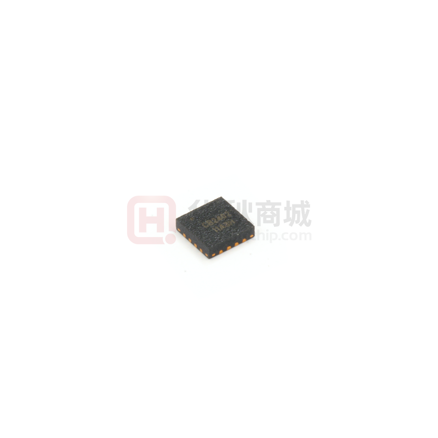
3 x 3 x 0.55mm Small Outline QFN-16 Package with
Exposed Ground Pad
APPLICATIONS
- 1 / 11 -
802.11b/g/n Embedded Applications
802.11b/g/n NIC PC Card
802.11b/g/n Multimedia Applications
802.11b/g/n Mobile Platforms
Other 2.4GHz Transceivers
802.11b/g/n Access Point
www.chipbetter.com
�PRELIMINARY
CB2402
2.4GHZ WLAN TRANSMIT/RECEIVE FEM
PIN-OUT DIAGRAM
15
16
1
GND
2
17
4
TX
13
GND
3
GND
14
DNC
6
5
TXEN
12
GND
11
GND
10
ANT
9
GND
NF
ID
EN
TI
RX
VDD
AL
GND
VDD
RXEN
7
8
DET
GND
Figure 2. CB2402 Pin out (Top View)
PIN ASSIGNMENTS
Name
RX
Description
Received RF Signal from the LNA to the Transceiver; DC Shorted to GND
2, 3, 8, 9,11,12, 15, 17
4
5
6
7
GND
TX
TXEN
RXEN
DET
Ground – Must be connected to Ground in the Application Circuit
Transmitted RF signal from the Transceiver to the PA: DC Shorted to GND
CMOS Input to Enable the PA
CMOS Input to Enable the LNA
Analog Voltage Proportional to the PA Power Output
Antenna port RF Signal from the PA or RF Signal Applied to the LNA; DC Shorted
to GND
Reserved – Do Not Connect in the Application Circuit
Voltage Supply Connection
DNC
VDD
CH
IP
BE
T
13
14,16
ANT
TE
R
10
CO
Pin
1
Chipbetter Microelectronics Inc.
- 2 / 11 -
www.chipbetter.com
�PRELIMINARY
CB2402
2.4GHZ WLAN TRANSMIT/RECEIVE FEM
CB2402 ABSOLUTE MAXIMUM RATINGS
Storage Ambient Temperature
Minimum
0
0
All Operating Modes
When RX is “ON”
No RF and DC Voltages Applied Appropriate
care required according to JEDEC Standards
Human Body Model
Maximum
4.5
3.6
350
1
+10
+5
Units
V
V
mA
uA
dBm
dBm
+150
°C
AL
Conditions
All VDD Pins
Through 1Kohm resistor
Through VDD Pins when TX is “ON”
NF
ID
EN
TI
Parameters
DC VDD Voltage Supply
DC Control Pin Voltage
DC VDD Current Consumption
DC Control Pin Current Consumption
TX RF Input Power
ANT RF Input Power
-50
ESD Voltage (HBM)
1000
V
NOTE:
Sustained operation at or above the Absolute Maximum Ratings for any single or combinations of the above parameters
may result in permanent damage to the device and is not recommended. All Maximum RF Input Power Ratings assume 50Ohm terminal impedance.
RECOMMENDED OPERATING CONDITIONS
Conditions
CO
All VDD Pins
All Operating Modes
Minimum
2.4
2.7
1.2
Typical
3.3
2.0
0
1
Maximum
2.5
3.6
VDD
0.3
5
0.8
50
-40
+85
Units
GHz
V
V
V
μA
μA
µsec
Ω
°C
CH
IP
BE
T
TE
R
Parameters
Operating Frequency
DC VDD Voltage Supply
Control Voltage “High”
Control Voltage “Low”
Control Pin Current Consumption
DC Shutdown Current
PA Turn On/Off Time
Input/Output Single-Ended Impedance
Operating Ambient Temperature
Chipbetter Microelectronics Inc.
- 3 / 11 -
www.chipbetter.com
�PRELIMINARY
CB2402
2.4GHZ WLAN TRANSMIT/RECEIVE FEM
CB2402 ELECTRICAL SPECIFICATIONS1
+20
16
POUT = +20dBm at ANT
2.525
-35
-35
-10
-10
50
-7
GHz
dBm
dBm
dBm
dBm
dB
dB
mA
mA
mV
dBc
dBc
dB
dB
Ohm
dBm
+22
+21
16
17
26
26.5
95
160
2500
All non-harmonically related spurs less
than -43 dBm/Hz
4:1
6:1
N/A
No damage
8:1
10:1
N/A
Parameters
Standby Mode:
DC Shutdown Current
TX-ANT Insertion Loss (S21)
TX Port Return Loss (S11)
ANT-RX Insertion Loss (S21)
RX Port Return Loss (S22)
Transmit-Receive Switching Time
Shut-Down and “ON” State Switching Time
Min
Test Condition
CH
Pin < -20dBm
From TX Port
Pin < -20dBm
From RX Port
- 4 / 11 -
Typ.
2.4
Max
Units
2.525
GHz
dB
dB
dB
dB
Ohm
mA
dBm
Max
Units
5
uA
dB
dB
dB
dB
ns
ns
10
3.5
-10
-10
50
10mA
2
TE
R
BE
T
Units
250
Min
IP
Max
2.4
Parameters
Test Condition
Receive Mode:(VDD=3.3V; T=+25℃)
Operating Frequency Band
All RF Pins Terminated by 50 Ohms
Gain
Noise Figure
Input Return Loss
Output Return Loss
RF Port Impedance
RX Quiescent Current
No RF Applied
Input P1dB
No RF Applied
Chipbetter Microelectronics Inc.
Typ.
NF
ID
EN
TI
All RF Pins Terminated by 50 Ohms
CW
1Mbps CCK, Mask Compliance
54Mbps OFDM, EVM< -33dB at ANT
54Mbps OFDM, EVM 1.2V)
2. “0” denotes low voltage stage (
很抱歉,暂时无法提供与“CB2402”相匹配的价格&库存,您可以联系我们找货
免费人工找货