PRELIMINARY
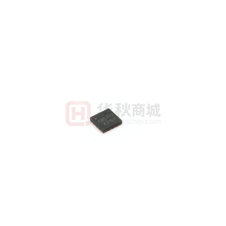
CB5717
5 GHz WLAN Front-End Module
DESCRIPTION
EN
TI
A
L
CB5717 is a highly integrated RF Front-End Integrated Circuit which incorporates key RF functionality needed for IEEE
802.11a/n/ac WLAN systems operating in the 5.15-5.9GHz range. CB5717 integrates a high-efficiency high-linearity power
amplifier (PA), a low noise amplifier (LNA) with bypass, the associated matching network, LO rejection, and harmonic filters all
in one device.
CB5717 has simple and low-voltage control logic, and requires minimal external components. A power detector is also
integrated for accurate monitoring of output power from the PA.
CB5717 is assembled in a compact, low-profile 2.5x2.5x0.55mm 16-lead QFN package. CB5717 is the ideal RF front-end
solution for implementing 5GHz high-power WLAN systems supporting multiple standards including 802.11ac.
RX
2
ANT
14
13
NF
ID
1
15
12 GND
11 VCC
CO
GND
GND
16
RX_EN
LNA_EN
BLOCK DIAGRAM
10 VCC
VDD
4
9
N/C
8
TX
7
GND
6
TE
R
5
TX_EN
3
VDET
GND
Figure 1. CB5717 Block Diagram
BE
T
FEATURES
Integrated high performance 5GHz PA, LNA with
bypass and T/R switch
Fully-matched input and output
Integrated power detector
Transmit gain: 28.5dB
Receive gain: 10dB
Output power: +20dBm @ 1.8% EVM,
VHT80/MCS9, 5V
Output power: +21dBm @ 3% EVM,
HT40/MCS7, 5V
Integrated 2.4GHz Notch Filter
ESD protection circuitry on all PINs
DC decoupled RF ports
Minimal external components required
Small package: QFN16 2.5mm x 2.5mm
x0.55mm (MSL3, 260℃ per JEDEC J-STD-020)
RoHS and REACH Compliant
IP
CH
APPLICATIONS
Chipbetter Microelectronics Inc.
- 1 / 11 -
802.11ac Wi-Fi Devices
Tablets / MIDs
Wi-Fi Media Gateways
Consumer Electronics s
Notebook / Netbook / Ultrabook
Access Points / Routers
Set Top Boxes / Wireless IPTVs
Other 5GHz ISM Platforms
www.chipbetter.com
�PRELIMINARY
CB5717
5 GHz WLAN Front-End Module
3
VDD
4
RX_EN
GND
ANT
AL
GND
13
12 GND
11 VCC
10 VCC
9
VDET
5
6
7
8
TX
2
14
NF
ID
EN
TI
RX
15
GND
1
16
TX_EN
GND
LNA_EN
PIN-OUT DIAGRAM
N/C
Figure 2. CB5717 Pin out (Top View)
Name
VDD
VDET
TX_EN
TX
NC
VCC
ANT
RX_EN
LNA_EN
Description
Ground – Must Be Connected to GND in the Application Circuit
RF Output Port from LNA or Bypass
LNA/Switch/Regulator Supply Voltage
Analog Voltage Proportional to the PA Power Output
Input to Control TX Enable
RF Input Port from the Transceiver
Internally Not Connected
PA Supply Voltage
Antenna Port RF Signal from the PA or RF Signal Applied to the LNA
Input to Control RX Enable
Input to Control LNA Enable or Bypass Mode
CH
IP
BE
T
4
5
6
8
9
10,11
13
15
16
GND
RX
TE
R
Pin
1,3,7,12,14
2
CO
PIN ASSIGNMENTS
Chipbetter Microelectronics Inc.
- 2 / 11 -
www.chipbetter.com
�PRELIMINARY
CB5717
5 GHz WLAN Front-End Module
ABSOLUTE MAXIMUM RATINGS
Test Condition
VDD and VCC
Minimum
4.5
2.0
0
Typical
5.0
3.0
Maximum
5.5
0.3
50
-40
85
Units
V
V
V
uA
°C
CH
IP
BE
T
TE
R
CO
Parameters
DC Supply Voltage
Control Pin Voltage “High”
Control Pin Voltage “Low”
Control Pin DC Current
Operation Temperature
NF
ID
RECOMMENDED OPERATING CONDITIONS
EN
TI
A
L
Parameters
Test Condition
Minimum
Maximum Units
DC Supply Voltage
VDD and VCC
0
6.0
V
Control Pin Voltage
All Control Pins
0
3.6
V
DC Current Consumption
600
mA
Input Power (50 ohm load)
+5
dBm
Storage Temperature
-40
150
°C
Operation Temperature
-40
85
°C
Junction Temperature
150
°C
ESD
All PINs, HBM
1000
V
NOTE:
Sustained operation at or above the Absolute Maximum Ratings for any one or combinations of the above parameters may
result in permanent damage to the device and is not recommended. All Maximum RF Input Power Ratings assume 50-ohm
terminal impedance.
Chipbetter Microelectronics Inc.
- 3 / 11 -
www.chipbetter.com
�PRELIMINARY
CB5717
5 GHz WLAN Front-End Module
CB5717 ELECTRICAL SPECIFICATIONS1
No Permanent Damage @ Pin =+10dBm
10:1
VSWR
CH
IP
BE
T
TE
R
Ruggedness
CO
NF
ID
EN
TI
A
L
Parameters
Symbol
Test Condition
Min
Typ.
Max
Units
Transmit Mode:(VDD=VCC= 5V, TX_EN=2.9V, RX_EN=LNA_EN=0V, T = 25℃, Unless Otherwise Noted)
Frequency
f
Main Frequency Band
5.15
5.90
GHz
Gain
G
26.0
28.5
dB
Gain Flatness
Over Any 80MHz Bandwidth
-0.5
+0.5
dB
With -45dB EVM source
VHT160/MCS9, 1.8% DEVM, Preamble only
+19.0 +19.5
VHT80/MCS9, 1.8% DEVM, Preamble only
Output Power
POUT
+19.5 +20.0
dBm
HT40/MCS7, 3% DEVM, Preamble Only
+20.0 +21.0
HT20/MCS0, Mask Compliance
+22.0 +23.0
CW Signal
Current
ICC
@ No RF
305
335
mA
Consumption
@+20dBm
340
375
HT20/MCS0 Signal @ +23dBm
dBm
Harmonics
2fo
2nd harmonics
-31
/MHz
3fo
3rd harmonics
-42
Isolation
ISO
From ANT to either TX or RX Pin
-27
-30
dB
Input Return Loss
|S11|
-14
-17
dB
Output Return Loss
|S22|
-12
-15
dB
VDET
@ No RF
0.25
0.30
Power Detector
V
Output
@+20dBm
0.35
0.40
PA Switching Time
tSW
ShutdownTX
400
500
ns
All non-harmonically related outputs less
Stability
6:1
VSWR
than -36dBm/MHz
Chipbetter Microelectronics Inc.
- 4 / 11 -
www.chipbetter.com
�PRELIMINARY
CB5717
5 GHz WLAN Front-End Module
EN
TI
A
L
Parameters
Symbol
Test Condition
Min
Typ.
Max
Units
Receive LNA Mode:(VDD=VCC= 5V, TX_EN=0V, RX_EN=LNA_EN=3V, T = 25℃, Unless Otherwise Noted)
Frequency
f
Main Frequency Band
5.15
5.90
GHz
Gain
G
8
10
dB
Input 1dB
Input
-2.0
-0.4
dBm
Compression Point
P1dB
Gain Flatness
Over any 80MHz Bandwidth
-0.5
+0.5
dB
Noise Figure
NF
3.5
4.0
dB
Input Return Loss
|S11|
-11
-13
dB
Output Return Loss
|S22|
L
-4
-6
dB
3rd Order Input
IIP3
0
dBm
Intercept Point
Switching Time
tSW
LNATX
800
ns
Current
IDD
@ No RF
15
25
mA
Consumption
TE
R
CO
NF
ID
Parameters
Symbol
Test Condition
Min
Typ.
Max
Units
Receive Bypass Mode:(VDD=VCC= 5V, TX_EN=LNA_EN=0V, RX_EN=3V, T = 25℃, Unless Otherwise Noted)
Frequency
f
Main Frequency Band
5.15
5.90
GHz
Insertion Loss
I.L.
9
12
dB
Input 1dB
Input
+8
dBm
Compression Point
P1dB
Input Return Loss
|S11|
-10
-12
dB
Output Return Loss
|S22|
-8
-10
dB
3rd Order Input
IIP3
+15
dBm
Intercept Point
Switching Time
tSW
Bypass LNA
100
200
ns
Current
IDD
@ No RF
13
18
uA
Consumption
LOGIC TRUTH TABLE
LNA_EN
0
0
1
0
All Others
RX_EN
0
0
1
1
CH
IP
BE
T
Mode
TX_EN
Shutdown Mode
0
Transmit Mode
1
LNA Low NF Receive Mode
0
Bypass Receive Mode
0
Unsupported
NOTE:
1. “1” denotes high voltage state (=3.0V);
2. “0” denotes low voltage state (
很抱歉,暂时无法提供与“CB5717”相匹配的价格&库存,您可以联系我们找货
免费人工找货