PRELIMINARY
CB6317
2496 to 2690 MHz Wide Instantaneous Bandwidth High-Efficiency
Power Amplifier
DESCRIPTION
AL
CB6317 is a high-efficiency, wide instantaneous bandwidth, fully input/output matched power amplifier (PA) with high gain and
linearity. The compact 5x5 mm PA is designed for FDD and TDD 4G LTE and 5G systems operating from 2496 to 2690 MHz.
The active biasing circuitry is integrated to compensate PA performance over temperature, voltage, and process variation.
BLOCK DIAGRAM
VCC1
NF
ID
EN
TI
A block diagram of the CB6317 is shown in Figure 1. The device package and pinout are shown in Figure 2.
VBIAS PAEN
VCC3
Active Bias
Input
Match
Stage1
PA
Stage2 Stage3
PA
PA
Output
Match
RFOUT
CO
RFIN
VCC2
Figure 1. CB6317 Block Diagram
FEATURES
FDD and TDD 4G LTE and 5G systems
Supports 3GPP Bands 7, 38, and 41
Driver amplifier for micro-base and macro-base
stations
Enterprise small cell and massive MIMO
BE
T
Wide instantaneous signal bandwidth: 100 MHz
High efficiency: PAE = 26% @ +28 dBm
High linearity: +28 dBm with < -45 dBc ACLR
with pre-distortion (100 MHz 5G,NR, 8.5 dB PAR
signal)
High gain: 34 dB
Excellent input and output return loss: to 50Ω
system
Integrated active bias: performance
compensated over temp
Integrated enable On/Off function: PAEN = 1.7 to
2.5 V
Single supply voltage: 5.0 V
Pin-to-pin compatible PA family supporting all
3GPP bands
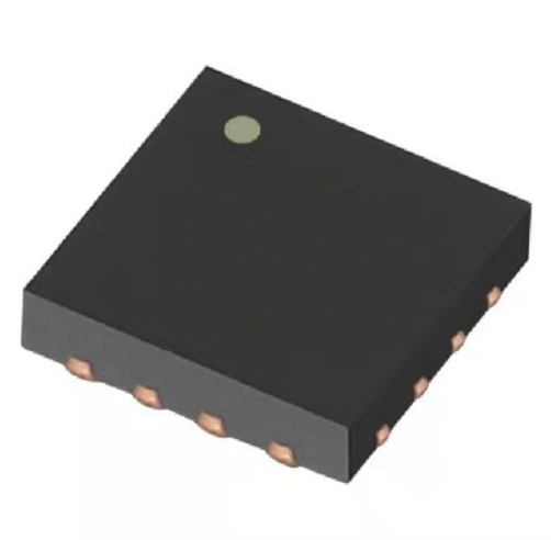
Compact (16-pin, 5 x 5 x 0.77 mm) package
(MSL3, 260℃ per JEDEC J-STD-020)
TE
R
APPLICATIONS
IP
CH
Chipbetter Microelectronics Inc.
- 1 / 10 -
www.chipbetter.com
�PRELIMINARY
CB6317
2496 to 2690 MHz Wide Instantaneous Bandwidth High-Efficiency
Power Amplifier
3
GND
4
VCC2
GND
GND
12 VCC3
AL
GND
13
NF
ID
EN
TI
2
14
11 GND
10 GND
9
VBAS
5
RFOUT
88
6
7
GND
RFIN
15
GND
1
16
PAEN
GND
VCC1
PIN-OUT DIAGRAM
PIN ASSIGNMENTS
Description
Ground
RF input port
Pin
9
10
Name
RFOUT
GND
Description
RF output port
Ground
GND
GND
VBIAS
PAEN
GND
GND
Ground
Ground
Bias voltage
PA enable
Ground
Ground
11
12
13
14
15
16
GND
VCC3
GND
VCC2
GND
VCC1
Ground
Stage 3 collector voltage
Ground
Stage 2 collector voltage
Ground
Stage 1 collector voltage
CH
IP
BE
T
3
4
5
6
7
8
Name
GND
RFIN
TE
R
Pin
1
2
CO
Figure 2. CB6317 Pin out (Top View)
Chipbetter Microelectronics Inc.
- 2 / 10 -
www.chipbetter.com
�PRELIMINARY
CB6317
2496 to 2690 MHz Wide Instantaneous Bandwidth High-Efficiency
Power Amplifier
ABSOLUTE MAXIMUM RATINGS
CO
NF
ID
EN
TI
AL
Parameters
Symbol
Minimum
Maximum Units
RF input power (CW, 50Ω load)
PIN
+10
dBm
Supply voltage (VCC1, VCC2, VCC3, VBIAS)
VCC
5.5
V
PA enable
VEN
2.8
V
Operating temperature
TC
-25
+115
°C
Storage temperature
TST
-55
+125
°C
Junction Temperature
TJ
+150
°C
Power dissipation
PD
1.3
W
Device thermal resistance
θJC
19.5
°C/W
Electrostatic discharge:
Charged Device Model (CDM)
500
V
Human Body Model (HBM)
1000
V
NOTE:
Exposure to maximum rating conditions for extended periods may reduce device reliability. There is no damage to device
with only one parameter set at the limit and all other parameters set at or below their nominal value. Exceeding any of the
limits listed here may result in permanent damage to the device.
ESD HANDLING:
Although this device is designed to be as robust as possible, electrostatic discharge (ESD) can
damage this device. This device must be protected at all times from ESD when handling or
transporting. Static charges may easily produce potentials of several kilovolts on the human body or
equipment, which can discharge without detection. Industry-standard ESD handling precautions
should be used at all times.
RECOMMENDED OPERATING CONDITIONS
Symbol
VCC1, VCC2, VCC3, VBIAS
PAEN
TE
R
Parameters
Supply voltage
PA enable:
ON
OFF
PA enable current
Operating frequency
Operating temperature
IENABLE
f
TC
Minimum
4.5
Typical
5
Maximum
5.25
Units
V
1.7
2.0
0
1
2.5
0.5
12
2690
+110
V
V
μA
MHz
℃
+25
CH
IP
BE
T
2496
-40
Chipbetter Microelectronics Inc.
- 3 / 10 -
www.chipbetter.com
�PRELIMINARY
CB6317
2496 to 2690 MHz Wide Instantaneous Bandwidth High-Efficiency
Power Amplifier
CB6317 ELECTRICAL SPECIFICATIONS1
CH
IP
BE
T
TE
R
CO
NF
ID
EN
TI
AL
Parameters
Symbol
Test Condition
Min
Typ.
Max
Units
Transmit Mode:(VCC1 = VCC2 = VCC3 = VBIAS = 5 V, PAEN = 2.0 V, f = 2593 MHz, TC = +25 ℃, Input/Output
Load = 50 Ω, Unless Otherwise Noted)
Frequency
f
2496
2690
MHz
Small signal gain
|S21|
PIN = -30 dBm
33.5
34
dB
Input return loss
|S11|
PIN = -30 dBm
28
dB
Output return loss
|S22|
PIN = -30 dBm
8
dB
Reverse isolation2
|S12|
PIN = -30 dBm
50
dB
ACLR @ raw dBm
ACLR
POUT = +28 dBm
-35
dBc
Output power at 1 dB gain
P1dB
CW, reference to small signal gain
+33.5
dBm
compression
Output power at 3 dB gain
P3dB
CW, reference to small signal gain
+35.5
dBm
compression
2nd harmonic
2fo
CW, POUT = +28 dBm
-45
dBc
3rd harmonic
3fo
CW, POUT = +28 dBm
-45
dBc
Power-added efficiency
PAE
CW, POUT = +28 dBm
27
%
Quiescent current
ICQ
No RF signal
140
mA
Load mismatch stress with no
VCC =+5 V, CW Pout = +28 dBm
6:1
VSWR
permanent degradation or failure
Measured from 50% PA enable
RF turn-on/turn-off time2
Ton
voltage level to 90% of RF
3
us
amplitude
NOTE:
1. Performance is guaranteed only under the conditions listed in this table.
2. RF turn-on time is measured from the time the PA enable reaches 50% of PA enable "on" level to the time at which the
RF output power achieves 90% of the average steady-state “on” level. RF turn-off time is measured from the time the
PA enable reaches 50% of PA enable "on" level to the time at which the RF output power decreases to 10% of the
average steady-state “on” level.
Chipbetter Microelectronics Inc.
- 4 / 10 -
www.chipbetter.com
�PRELIMINARY
CB6317
2496 to 2690 MHz Wide Instantaneous Bandwidth High-Efficiency
Power Amplifier
EVALUATION BOARD SCHEMATIC
C9
C5
C7
C10
VCC2
C13
GND7
VCC2
GND8
GND6
RFIN
GND5
GND1
8
7
6
5
4
3
2
1
PAEN
VBIAS
C2
VBIAS
C3
VCC1
VCC2
VCC3
PAEN
C11
C14
VCC3
SMA
C4
CO
Header 8
C8
J8
GND4
RFOUT
GND3
GND2
C6
12
11
10
9
5
6
7
8
SMA
VCC3
GND
PAEN
C1
GND_PAD
VBIAS
J7
17
1
2
3
4
VCC1
16
15
14
13
C12
NF
ID
EN
TI
VCC1
AL
The CB6317 Evaluation Board is used to test the performance of the CB6317 PA. An Evaluation Board
schematic is provided in Figure 3
CH
IP
BE
T
TE
R
Figure 3. CB6317 Evaluation Board Schematic
Chipbetter Microelectronics Inc.
- 5 / 10 -
www.chipbetter.com
�PRELIMINARY
CB6317
2496 to 2690 MHz Wide Instantaneous Bandwidth High-Efficiency
Power Amplifier
CO
NF
ID
EN
TI
AL
EVALUATION BOARD ASSEMBLY DRAWING
Figure 4. CB6317 Evaluation Board Assembly Drawing
TE
R
BILL OF MATERIALS
Value
100pF
4.7nF
1uF
0.47uF
0.22uF
10uF
Size
0402
0402
0402
0402
0402
1206
Vendor
Murata
Murata
Murata
Murata
Murata
Murata
Part Number
GRT1555C1E101JA02D
GRM155R71C472KA01D
GRM155R60J105KE19D
GRM155R61E474KE01D
GRM155C81E224KE01D
GRM155R60J106ME44D
CH
IP
BE
T
Component
C1, C2
C4
C3
C5, C7, C8
C6
C9,C10,C11
Chipbetter Microelectronics Inc.
- 6 / 10 -
www.chipbetter.com
�PRELIMINARY
CB6317
2496 to 2690 MHz Wide Instantaneous Bandwidth High-Efficiency
Power Amplifier
PCB LAND PATTERN
16X0.5mm
Pin 1 Indicator 0.20X45°
16X0.67mm
NF
ID
EN
TI
9XФ0.875mm
Stencil aperture size for
center grund pad shuld be
80% to 100%(by area) for the
solder mask opening
5.3mm
Pin 1
AL
5.3mm
Pin 16
0.8mm Pitch
Package Outline
0.125mm Typ
Stencil Aperture
Top View
Pin 16
5.3mm
0.6mm Pitch
Pin 16
Pin 1 Indicator 0.20X45°
7X0.67 mm
Pin 1
7X0.5mm
0.6 mm Pitch
5.4mm
16X0.6mm
16X0.77mm
Pin 1
5.4mm
Themal via array Ф0.03 mm
0.6mm Pitch improves themal
performance
CO
5.3 mm
0.8mm Pitch
2X1.4375 mm
Package Outline
Package Outline
0.8mm Pitch
0.25mm Typ
Opening size of 60% to 100% of
exposed center opening shown
2X1.4375 mm
Solder Mask Opening
Top View
TE
R
Metallization
Top View
CH
IP
BE
T
Figure 7. CB6317 PCB Layout Footprint
Chipbetter Microelectronics Inc.
- 7 / 10 -
www.chipbetter.com
�PRELIMINARY
CB6317
2496 to 2690 MHz Wide Instantaneous Bandwidth High-Efficiency
Power Amplifier
Pin 1
Indicator
CB6317
XXXXXX
YYWW
NF
ID
EN
TI
Part Number
AL
TYPICAL PART MARKING
ChipBetter Lot Code
Data Code:
YY=Calendar
Year
WW=Work Week
Figure 6. Typical Part Marking for the CB6317
PACKAGE DIMENSIONS (All Dimensions in mm):
16xSMT Pad
Solder Mask Opening
0.2 A B C
C
TE
R
6x1
8x2.4
BE
T
4x1.2
A
0.1
Top View
Bottom View
Side View
0.875
0.875
0.42±0.1
0.20x45°
4XR0.05Max
0.5±0.05 0.6±0.05
IP
CH
0
6x1
See Detail A
0.15 A B C
Detail A
SMT Pad
Scale:2X
4X This Rotation
4X Rotated 180°
4X Rotated 90°CW
4X Rotated 90°CCW
Pin 1
A
See Detail B
0.77±0.1
Metal Pad Edges
4x1.2
4x0.4
5
(0.1)
Solder Mask Edage
Solder Mask Edge
Pin 16
Pin 1 Indicator
See Detail C
0
Top
4x0.4
Pin 1
Indicator
6x1
B
0.875
5
A B C
CO
0.1
Detail B
Pad
Scale:2X
8X this rotation
Solder Mask Edage
5XR0.05 Max
0.875
Detail C
Pad
Scale:2X
1X this rotation
Notes:
1. Dimensions are in millimeters (unless otherwise
specified).
2. Dimensions and tolerances are in accordance with
ASME Y14.5M-1994
Chipbetter Microelectronics Inc.
Figure 8. CB6317 Package Dimension
- 8 / 10 -
www.chipbetter.com
�PRELIMINARY
CB6317
2496 to 2690 MHz Wide Instantaneous Bandwidth High-Efficiency
Power Amplifier
0.25±0.20
Ф1
.50
+
2.00±0.10
0.1
0
4.00±0.10
5.50±0.10
12.00±0.20
NF
ID
EN
TI
5.25±0.10
Pin 1
1.75±0.10
AL
TAPE AND REEL DIMENSIONS
1.4±0.10
8.00±0.10
Ф1.50+0.10
CO
5.25±0.10
Notes:
1.
Carrier tapes must meet all requirements of Chipbetter spec for tape and reel shipping.
2.
Carrier tape shall be black conductive polycarbonate.
3.
Cover tape shall be transparent conductive material.
4.
ESD-surface resistivity shall be ≤ 1 × 10¹⁰ Ω/square per EJA, JEDEC TNR specification.
5.
All measurements are in millimeters.
CH
IP
BE
T
TE
R
Figure 9. CB6317 Tape and Reel Dimensions
Chipbetter Microelectronics Inc.
- 9 / 10 -
www.chipbetter.com
�PRELIMINARY
CB6317
2496 to 2690 MHz Wide Instantaneous Bandwidth High-Efficiency
Power Amplifier
CONTACT INFORMATION
For the latest specifications, additional product information, worldwide sales and distribution locations:
AL
Web: www.chipbetter.com
Tel: 0755-26654180
NF
ID
EN
TI
DISCLAIMERS
ChipBetter reserves the right to make changes without further notice to specifications and product descriptions in this
document to improve reliability, function or design. ChipBetter does not assume any liability arising out of the application
or use of information or product described in this document. Neither does ChipBetter convey any license under its
intellectual property rights nor licenses to any of circuits described in this document to any third party.
The information in this document is believed to be accurate and reliable and is provided on an "as is" basis, without any
express or implied warranty. Any information given in this document does not constitute any warranty of merchantability
or fitness for a particular use. The operation of this product is subject to the user's implementation and design practices.
ChipBetter products are not designed or intended for use in life support equipment, devices or systems, or other critical
applications, and are not authorized or warranted for such use.
CH
IP
BE
T
TE
R
CO
Copyright of ChipBetter Microelectronics Co, Ltd. All rights reserved.
Chipbetter Microelectronics Inc.
- 10 / 10 -
www.chipbetter.com
�
很抱歉,暂时无法提供与“CB6317”相匹配的价格&库存,您可以联系我们找货
免费人工找货