PRELIMINARY
CB6318
3300 to 3600 MHz Wide Instantaneous Bandwidth High-Efficiency
Power Amplifier
DESCRIPTION
AL
CB6318 is a highly efficient, wide instantaneous bandwidth, fully input/output matched power amplifier (PA) with high gain and
linearity. The compact 5x5 mm PA is designed for FDD and TDD 4G LTE and 5G systems operating from 3300 to 3600 MHz.
The active biasing circuitry is integrated to compensate PA performance over temperature, voltage, and process variation.
BLOCK DIAGRAM
VCC1
Input
Match
RFIN
NF
ID
EN
TI
A block diagram of the CB6318 is shown in Figure 1. The device package and pin out are shown in Figure 2.
VCC2
Stage 1
VCC3
Stage 2
Stage 3
Output
Match
RFOUT
Bias Circuits
Vbias
CO
PAEN
Figure 1. CB6318 Block Diagram
FEATURES
5G and 4G FDD and TDD systems
Supports 3GPP and 5G Bands 22, 42, n77, and n78
Driver amplifier for micro-base and macro-base
stations
Enterprise small cell and massive MIMO
BE
T
Wide instantaneous signal bandwidth: 100 MHz
High efficiency: PAE = 22%~23% @ +28 dBm
High gain: 36 dB
Excellent input and output return loss: to 50Ω
system
Integrated active bias: performance
compensated over temp
Integrated enable On/Off function: PAEN = 1.7 to
3V
Single supply voltage: 5.0 V
Pin-to-pin compatible PA family supporting major
3GPP bands
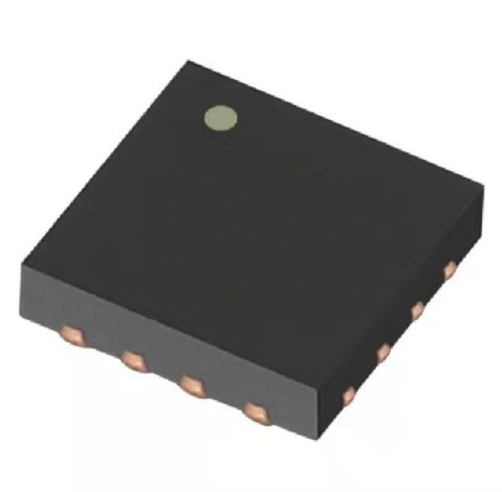
Compact (16-pin, 5 x 5 x 1.1 mm) package
(MSL3, 260℃ per JEDEC J-STD-020)
TE
R
APPLICATIONS
CH
IP
Chipbetter Microelectronics Inc.
- 1 / 10 -
www.chipbetter.com
�PRELIMINARY
CB6318
3300 to 3600 MHz Wide Instantaneous Bandwidth High-Efficiency
Power Amplifier
3
GND
4
VCC2
GND
GND
12 VCC3
AL
GND
13
NF
ID
EN
TI
2
14
11 GND
10 GND
9
VBAS
5
RFOUT
88
6
7
GND
RFIN
15
GND
1
16
PAEN
GND
VCC1
PIN-OUT DIAGRAM
PIN ASSIGNMENTS
Description
Ground
RF input port
Pin
9
10
Name
RFOUT
GND
Description
RF output port
Ground
GND
GND
VBIAS
PAEN
GND
GND
Ground
Ground
Bias voltage
PA enable
Ground
Ground
11
12
13
14
15
16
GND
VCC3
GND
VCC2
GND
VCC1
Ground
Stage 3 collector voltage
Ground
Stage 2 collector voltage
Ground
Stage 1 collector voltage
CH
IP
BE
T
3
4
5
6
7
8
Name
GND
RFIN
TE
R
Pin
1
2
CO
Figure 2. CB6318 Pin out (Top View)
Chipbetter Microelectronics Inc.
- 2 / 10 -
www.chipbetter.com
�PRELIMINARY
CB6318
3300 to 3600 MHz Wide Instantaneous Bandwidth High-Efficiency
Power Amplifier
ABSOLUTE MAXIMUM RATINGS
CO
NF
ID
EN
TI
AL
Parameters
Symbol
Minimum
Maximum
Units
RF input power (CW, 50Ω load)
PIN
+16
dBm
Supply voltage (VCC1, VCC2, VCC3, VBIAS)
VCC
5.5
V
PA enable
VEN
1.7
3
V
Operating temperature
TC
-40
+110
°C
Storage temperature
TST
-55
+125
°C
Junction Temperature
TJ
+150
°C
Power dissipation (TCASE = 100°C): POUT = +28 dBm PDISS_28dBm
2.3
W
Device thermal resistance (TCASE = 100°C): POUT =
RTH28dBm
16.5
°C/W
+28 dBm
Electrostatic discharge:
Charged Device Model (CDM)
PIN
1000
V
Human Body Model (HBM)
1000
V
NOTE:
Exposure to maximum rating conditions for extended periods may reduce device reliability. There is no damage to device
with only one parameter set at the limit and all other parameters set at or below their nominal value. Exceeding any of the
limits listed here may result in permanent damage to the device.
ESD HANDLING:
Although this device is designed to be as robust as possible, electrostatic discharge (ESD) can
damage this device. This device must be protected at all times from ESD when handling or
transporting. Static charges may easily produce potentials of several kilovolts on the human body or
equipment, which can discharge without detection. Industry-standard ESD handling precautions
should be used at all times.
RECOMMENDED OPERATING CONDITIONS
Symbol
VCC1, VCC2, VCC3, VBIAS
PAEN
Minimum
4.75
1.7
TE
R
Parameters
Supply voltage
PA enable:
ON
OFF
PA enable current
Operating frequency
Operating temperature
IENABLE
f
TC
0
1
+25
Maximum
5.25
Units
V
3
0.5
202
3600
+110
V
V
μA
MHz
℃
CH
IP
BE
T
3300
-40
Typical
5
Chipbetter Microelectronics Inc.
- 3 / 10 -
www.chipbetter.com
�PRELIMINARY
CB6318
3300 to 3600 MHz Wide Instantaneous Bandwidth High-Efficiency
Power Amplifier
CB6318 ELECTRICAL SPECIFICATIONS1
CH
IP
BE
T
TE
R
CO
NF
ID
EN
TI
AL
Parameters
Symbol
Test Condition
Min
Typ.
Max
Units
Transmit Mode:(VCC1 = VCC2 = VCC3 = VBIAS = 5 V, PAEN = 2.0 V, f = 2593 MHz, TC = +25 ℃, Input/Output
Load = 50 Ω, Unless Otherwise Noted)
Frequency
f
3300
3600
MHz
Small signal gain
|S21|
PIN = -30 dBm
33
34.8
dB
Gain @ +23 dBm
|S21|@ +28 dBm
POUT = +28 dBm
35
36
dB
Input return loss
|S11|
PIN = -20 dBm
14
16
dB
Output return loss
|S22|
PIN =-20 dBm
9
10
dB
Reverse isolation2
|S12|
PIN =-30 dBm
58
dB
ACLR @ +28 dBm
ACLR
POUT = +28 dBm (After DPD)
-50
-47
dBc
Output power at 1 dB gain
CW, reference to small signal
P1dB
+34
+35
dBm
Compression2
gain (Pin= -30dBm)
Output power at 3 dB gain
CW, reference to small signal
P3dB
+35
+36
dBm
Compression2
gain (Pin= -30dBm)
2nd harmonic
2fo
CW, POUT = +28 dBm
-49
-42
dBc
3rd harmonic
3fo
CW, POUT = +28 dBm
-50
dBc
Power-added efficiency
PAE
CW, POUT = +28 dBm
20
22
%
Quiescent current
ICQ
No RF signal
102
mA
Measured from 50% PA enable
RF turn-on/turn-off time3
Ton
voltage level to 90% of RF
很抱歉,暂时无法提供与“CB6318”相匹配的价格&库存,您可以联系我们找货
免费人工找货