PRELIMINARY
CBG9326
GaAs HBT MMIC DRIVER AMPLIFIER, 3.0 - 4.5 GHz
DESCRIPTION
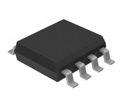
The device is provided in an EMSOP8 package.
BLOCK DIAGRAM
VPD
1
GND
2
RFIN
3
GND
4
NF
ID
EN
TI
AL
The CBG9326 is high efficiency GaAs HBT MMIC driver amplifier which operates between 3.0 and 4.5 GHz. The amplifier is
packaged in a low cost, surface mount 8 leaded package with an exposed base for improved RF and thermal performance.
The amplifier provides 19 dB of gain and +25 dBm of saturated power from a +3.3V supply voltage,and 23dB of gain and
+26dBm of saturated power from a +5V supply voltage. Power down capability is available to conserve current consumption
when the amplifier is not in use. Internal circuit matching was optimized to provide greater than 40% PAE.
RX OUT
8
VCC
7
GND
6
RFOUT
5
GND
CO
GND
TE
R
Figure 1. CBG9326 Block Diagram
FEATURES
Psat Output Power: +26 dBm
PAE > 40%
Output IP3: +32 dBm
High Gain: 24 dB
Vs: +5V
Ultra-Small Package: EMSOP8 (MSL1, 260℃
per JEDEC J-STD-020)
Microwave Radios
Broadband Radio Systems
Wireless Local Loop Driver Amplifier
CH
IP
BE
T
APPLICATIONS
Chipbetter Microelectronics Inc.
- 1 / 10 -
www.chipbetter.com
�PRELIMINARY
CBG9326
GaAs HBT MMIC DRIVER AMPLIFIER, 3.0 - 4.5 GHz
RX OUT
VCC
2
7
GND
RFIN
3
6
RFOUT
GND
4
5
GND
1
GND
NF
ID
EN
TI
8
VPD
AL
PIN-OUT DIAGRAM
GND
Figure 2. CBG9326 Pin out (Top View)
PIN ASSIGNMENTS
Description
Control Voltage
Ground
Pin
5
6
Name
GND
RFOUT
Description
Ground
RF Output Power
3
RFIN
RF Input Power
7
GND
Ground
4
GND
Ground
8
VCC
Collector Bias Voltage
CO
Name
VPD
GND
CH
IP
BE
T
TE
R
Pin
1
2
Chipbetter Microelectronics Inc.
- 2 / 10 -
www.chipbetter.com
�PRELIMINARY
CBG9326
GaAs HBT MMIC DRIVER AMPLIFIER, 3.0 - 4.5 GHz
ABSOLUTE MAXIMUM RATINGS
Parameters
Collector Bias Voltage (Vcc)
Control Voltage Range (Vpd)
VCC
VPD
PIN
Symbol
Min
Max
+5.5
+5.5
+15
Units
V
V
dBm
CH
IP
BE
T
TE
R
CO
NF
ID
EN
TI
AL
RF Input Power (RFIN)(Vs = Vpd = +5Vdc)
Supply current
ICC
800
mA
Storage temperature
Tst
-40
+150
°C
Operating Temperature
TC
-40
+85
Junction Temperature
TJ
+150
°C
Continuous Pdiss (T = 85 °C) (derate 14 mW/°C above 85 °C)
0.92
W
Electrostatic discharge: Human Body Model (HBM)
1000
V
NOTE:
Exposure to maximum rating conditions for extended periods may reduce device reliability. There is no damage to device
with only one parameter set at the limit and all other parameters set at or below their nominal value. Exceeding any of the
limits listed here may result in permanent damage to the device.
ESD HANDLING:
Although this device is designed to be as robust as possible, electrostatic discharge (ESD) can
damage this device. This device must be protected at all times from ESD when handling or
transporting. Static charges may easily produce potentials of several kilovolts on the human body or
equipment, which can discharge without detection. Industry-standard ESD handling precautions
should be used at all times.
Chipbetter Microelectronics Inc.
- 3 / 10 -
www.chipbetter.com
�PRELIMINARY
CBG9326
GaAs HBT MMIC DRIVER AMPLIFIER, 3.0 - 4.5 GHz
CBG9326 ELECTRICAL SPECIFICATIONS1
Parameters
Symbol
Test Condition
(TC = +25℃, Input/Output Load = 50 Ω, Unless Otherwise Noted)
Frequency
f
Main frequency band
Input return loss
|S11|
Output return loss
|S22|
Output Power for 1dB
Compression
P1dB
Saturated Output Power
Psat
PAE@Psat
Output Third Order Intercept
Noise Figure
PAE
IP3
NF
Pin = -30dBm
Pin = -30dBm
CW, Pin =8dBm
Vpd = 0V
Icq
Vpd = 3.3V/Vcc = 3.3V
Vpd = 5V/Vcc = 5V
MHz
20
21.5
5V
21
24
28
3.3V
9
5V
11
3.3V
7
5V
6
dB
dB
23
24
5V
21
24
3.3V
24
25
25.5
27
35
42
30.5
5
Ipd
tON/tOFF
dB
dBm
dBm
50
%
dBm
dB
0
1
uA
20
25
mA
90
95
7
10
mA
mA
ns
CH
IP
BE
T
TE
R
Control Current
Switching time
4500
16
5V
@Psat
Units
3.3V
CW, Reference to small signal
gain
3.3V
CO
Supply Current
Pin = -30dBm
3000
Max
AL
G
Typ.
NF
ID
EN
TI
Gain
Min
Chipbetter Microelectronics Inc.
- 4 / 10 -
www.chipbetter.com
�PRELIMINARY
CBG9326
GaAs HBT MMIC DRIVER AMPLIFIER, 3.0 - 4.5 GHz
PERFORMANCE PLOTS
(Test conditions unless otherwise noted: Temp. = +25 °C, Input/Output Load = 50 Ω)
Gain
30
3.3V
5V
-10
-15
-20
3.00
24
21
18
3.25
3.50
3.75
4.00
4.25
4.50
Frequency (GHz)
15
3.00
3.25
3.50
4.25
4.50
10
3.3V
5V
CO
3.3V
5V
-5
Noise
8
-10
6
4
TE
R
-15
-20
3.00
3.25
3.50
3.75
4.00
4.25
2
4.50
0
3.00
BE
T
Frequency (GHz)
P1dB
3.25
3.50
3.75
4.00
4.25
4.50
Frequency(GHz)
Psat
30
30
3.3V
5V
3.3V
5V
28
Psat (dBm)
IP
25
P1dB (dBm)
4.00
Noise Figure
0
CH
3.75
Frequency (GHz)
Output Return Loss
Output Return Loss (dB)
NF
ID
EN
TI
-5
3.3V
5V
27
Gain(dB)
Input Return Loss (dB)
0
AL
Input Return Loss
20
26
24
15
22
10
3.00
3.25
3.50
3.75
4.00
4.25
20
3.00
4.50
Frequency (GHz)
Chipbetter Microelectronics Inc.
3.25
3.50
3.75
4.00
4.25
4.50
Frequncy (GHz)
- 5 / 10 -
www.chipbetter.com
�PRELIMINARY
CBG9326
GaAs HBT MMIC DRIVER AMPLIFIER, 3.0 - 4.5 GHz
U3
1
2
3
4
VCC
VPD
GND
CBG9326
GND
RFOUT
RFIN
GND
GND
9
2
1
3
2
GND
VPD
1 R1
0R
VCC
C1
330pF
8
C2
330pF
L1
5.1nH
C5
2.2uF
7
6
C4
5
C3
0.7pF
4pF
3
VPD
2
1
2
3
4
5
6
7
8
9
10
NF
ID
EN
TI
VCC
AL
EVALUATION BOARD SCHEMATIC
1
U2
CH
IP
BE
T
TE
R
CO
Figure 3. CBG9326 Evaluation Board Schematic
Chipbetter Microelectronics Inc.
- 6 / 10 -
www.chipbetter.com
�PRELIMINARY
CBG9326
GaAs HBT MMIC DRIVER AMPLIFIER, 3.0 - 4.5 GHz
NF
ID
EN
TI
AL
EVALUATION BOARD ASSEMBLY DRAWING
Figure 4. CBG9326 Evaluation Board Assembly Drawing
BILL OF MATERIALS
Value
330pF
330pF
0.7pF
4pF
2.2 μF
5.1nH
Size
0402
0402
0402
0402
0805
0402
CO
Component
Vendor
Murata
Murata
Murata
Murata
Murata
Murata
Part Number
CH
IP
BE
T
TE
R
C1
C2
C3,
C4
C5
L1
Chipbetter Microelectronics Inc.
- 7 / 10 -
www.chipbetter.com
�PRELIMINARY
CBG9326
GaAs HBT MMIC DRIVER AMPLIFIER, 3.0 - 4.5 GHz
PCB LAND PATTERN
4.40
0.45
1.45
1.75
2.40
0.00
0.00
3.60
Land X1
Land Y1
Tab Land X2
Tab Land Y2
Silkscreen R1
Silkscreen R2
Courtyard V1
Courtyard V2
2
3
AL
2
3
4
5
6
7
8
9
1
8
9
7
6
NF
ID
EN
TI
Dimensions
1
B
X1
A
X2
Y2
Y1
4
5
C
CH
IP
BE
T
TE
R
CO
Figure 5. CBG9326 PCB Layout Footprint
Chipbetter Microelectronics Inc.
- 8 / 10 -
www.chipbetter.com
�PRELIMINARY
CBG9326
GaAs HBT MMIC DRIVER AMPLIFIER, 3.0 - 4.5 GHz
TYPICAL PART MARKING
CBG9326
XXXXXX
YYWWVC
AL
Pin 1
Indicator
Part Number
NF
ID
EN
TI
ChipBetter Lot Code
Data Code:
YY=Calendar
Year
WW=Work Week
Figure 6. Typical Part Marking for the CBG9326
PACKAGE DIMENSIONS (All Dimensions in mm):
1
P
CH
7
6
5
L
A
H
T
K
.031 0.80
.016 0.40
.200 5.08
.184 4.68
.070[1.78]
MAX
3
EXPOED GROUND PADDLE
MUST BE CONNECTED TO
RF/DC GROUND
.037 0.95
.029 0.75
.043[1.10]
MAX
9
4
IP
.122 3.10
.114 2.90
2
3
8°
0°
4
BE
T
.122 3.10
.114 2.90
8
Tt
W
TE
R
L
T
W
Tt
Wt
A
B
M
K
Wt
Y1
B
Pin Cout
0.65
8
8
Min
Max
4.68 5.08
0.40 0.80
0.22 0.38
2.41
1.78
2.90 3.10
2.90 3.10
1.10
0.00
CO
Pitch (P)
Pin Package
.005 0.13
.000 0.00
.0256[0.65] TYP
.015 0.38
.009 0.22 TYP
.009 0.22
.003 0.08
.095[2.41]
MAX
NOTES:
1. LEADFRAME MATERIAL: COPPER ALLOY
2. DIMENSIONS AREIN INCHES [MILLIMETERS]
3. DIMENSION DOES NOT INCLUDE MOLDFLASH OF 0.15mm PER SIDE
4. DIMENSION DOES NOT INCLUDE MOLDFLASH OF 0.25mm PER SIDE
5. ALL GROUND LEADS AND GROUND PADDLE MUST BE SOLDERED TO
PCB RF GROUND
Figure 7. CBG9326 Package Dimension
Chipbetter Microelectronics Inc.
- 9 / 10 -
www.chipbetter.com
�PRELIMINARY
CBG9326
GaAs HBT MMIC DRIVER AMPLIFIER, 3.0 - 4.5 GHz
CONTACT INFORMATION
For the latest specifications, additional product information, worldwide sales and distribution locations:
AL
Web: www.chipbetter.com
Tel: 0755-26654180
NF
ID
EN
TI
DISCLAIMERS
ChipBetter reserves the right to make changes without further notice to specifications and product descriptions in this
document to improve reliability, function or design. ChipBetter does not assume any liability arising out of the application
or use of information or product described in this document. Neither does ChipBetter convey any license under its
intellectual property rights nor licenses to any of circuits described in this document to any third party.
The information in this document is believed to be accurate and reliable and is provided on an "as is" basis, without any
express or implied warranty. Any information given in this document does not constitute any warranty of merchantability
or fitness for a particular use. The operation of this product is subject to the user's implementation and design practices.
ChipBetter products are not designed or intended for use in life support equipment, devices or systems, or other critical
applications, and are not authorized or warranted for such use.
CH
IP
BE
T
TE
R
CO
Copyright of ChipBetter Microelectronics Co, Ltd. All rights reserved.
Chipbetter Microelectronics Inc.
- 10 / 10 -
www.chipbetter.com
�
很抱歉,暂时无法提供与“CBG9326”相匹配的价格&库存,您可以联系我们找货
免费人工找货