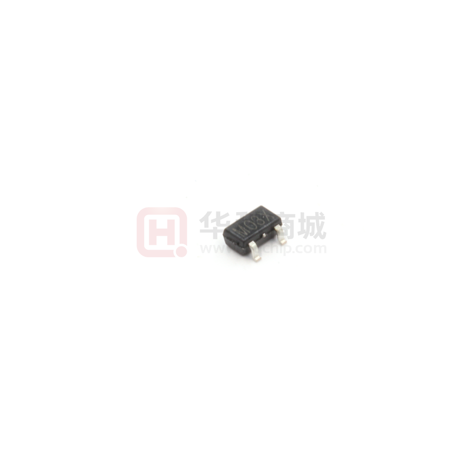
SSP61C series
Low Power Voltage Detector
Features
Low power consumption
High input voltage (up to 8V)
Low temperature coefficient
Output voltage accuracy: tolerance ±1% or ±2%
Built-in hysteresis characteristic
SOT23-3 and SOT23 package
Applications
Battery checkers
Microcomputer reset
Level selectors
Battery memory backup
Power failure detectors
Non-volatile RAM signal storage protectors
General Description
The SSP61C series devices are a set of three
in CMOS technology. Each voltage detector in the
series detects a particular fixed voltage ranging
inverter or NMOS open drain). CMOS technology
ensures low power consumption.
Although designed primarily as fixed voltage
detectors, these devices can be used with external
PR
O
from 0.9V to 5.0V. The voltage detectors consist of
IN
terminal low power voltage detectors implemented
hysteresis circuit, and an output driver (CMOS
a high-precision and low power consumption
components to detect user specified threshold
standard voltage source as well as a comparator,
voltages.
Selection Table
Part No.
Hys. Width
Output
Tolerance
0.9V
4%
CMOS
±1% or ±2%
SI
SSP61CC0902MR
Det. Voltage
SSP61CN0902MR
0.9V
4%
NMOS
±1% or ±2%
SSP61CC1002MR
1.0V
4%
CMOS
±1% or ±2%
SSP61CN1002MR
1.0V
4%
NMOS
±1% or ±2%
SSP61CC1102MR
1.1V
4%
CMOS
±1% or ±2%
SSP61CN1102MR
1.1V
4%
NMOS
±1% or ±2%
SSP61CC1202MR
1.2V
4%
CMOS
±1% or ±2%
SSP61CN1202MR
1.2V
4%
NMOS
±1% or ±2%
…
…
4%
…
±1% or ±2%
SSP61CC5002MR
5.0V
4%
CMOS
±1% or ±2%
SSP61CN5002MR
5.0V
4%
NMOS
±1% or ±2%
Ver1.2
1
Package
SOT23-3
SOT23
Shanghai Siproin Microelectronics Co.
�SSP61C series
Low Power Voltage Detector
Order Information
SSP61C①②③④⑤⑥⑦
Designator
②③
④⑤
⑥
⑦
Description
C
CMOS output
N
NMOS output
VOUT
Output Voltage(0.9~5.0V)
02
±2% accuracy
01
±1% accuracy
M
Package:SOT23-3
N
Package:SOT23
R
RoHS / Pb Free
G
Halogen Free
SI
PR
O
Block Diagram
IN
①
Symbol
Typical Application Circuits
Ver1.2
2
Shanghai Siproin Microelectronics Co.
�SSP61C series
Low Power Voltage Detector
Output Table & Curve
VDD>VDET(+)
Hi-Z
VDD≤VDET(-)
VSS
PR
O
IN
VDD
VOUT
SI
Pin Assignment
Ver1.2
3
Shanghai Siproin Microelectronics Co.
�SSP61C series
Low Power Voltage Detector
SI
PR
O
IN
Marking Rule
Ver1.2
4
Shanghai Siproin Microelectronics Co.
�SSP61C series
Low Power Voltage Detector
Absolute Maximum Ratings
Supply Voltage ................................-0.3V to 8V
Storage Temperature ..................-50℃ to 125℃
Operating Temperature .................-40℃ to 85℃
Note: These are stress ratings only. Stresses exceeding the range specified under “Absolute Maximum
Ratings” may cause substantial damage to the device. Functional operation of this device at other
conditions beyond those listed in the specification is not implied and prolonged exposure to extreme
conditions may affect device reliability.
Thermal Information
Symbol
Parameter
Package
Max.
θJA
Thermal Resistance (Junction to
Ambient) (Assume no ambient
airflow, no heat sink)
SOT23-3
500
SOT23-3
0.20
PD
Power Dissipation
Unit
℃/W
IN
W
PR
O
Note: PD is measured at Ta= 25℃
Electrical Characteristics
VDF=0.8V~5.0V
Ta=25℃
Parameter
Test Conditions
Min.
Typ.
Max.
Unit
VDET
Detection Voltage
VDF=0.8V~5.0V
VDF*0.98
VDF
VDF*1.02
V
VHYS
Hysteresis Width
-
0.02*VDET
0.05*VDET
0.10*VDET
V
Vin=1.5V
-
0.7
2.3
Vin=2.0V
-
0.8
2.7
Vin=3.0V
-
0.9
3.0
Vin=4.0V
-
1.0
3.2
Vin=5.0V
-
1.1
3.6
SI
Symbol
IDD
Operating Current
μA
VDD
Operating Voltage
-
-
0.7
-
10
V
IOL
Output Sink Current
2V
VOUT=0.2V
0.5
1
-
mA
∆VDET
VDF ∆Ta
Temperature
-
±100
-
ppm/℃
Ver1.2
Coefficient
-
-25℃
很抱歉,暂时无法提供与“SSP61CN2002MR”相匹配的价格&库存,您可以联系我们找货
免费人工找货- 国内价格
- 5+0.50728
- 50+0.40101
- 150+0.34787
- 500+0.28646
- 3000+0.25271
- 6000+0.23784
- 国内价格
- 10+0.44152
- 100+0.34902
- 600+0.25468
- 1200+0.25086
- 3000+0.22468
- 国内价格
- 1+0.46530
- 200+0.30030
- 1500+0.26070
- 3000+0.23100
