RY6050-ADJM5R
500mA Adjustable High-Speed Low Power LDO
Features
•
•
•
•
•
•
Programmable Output: Minimum can go to 0.8V
Low Power Consumption: 28μA (Typ.)
Low Voltage Drops: 0.15V@50mA
Standby Mode: less than 0.1uA
Low Temperature Coefficient
Active Discharge Function
•
•
•
•
•
High Ripple Rejection: 70dB@1KHz (Typ.)
High Input Voltage (up to 8V)
Output Voltage Accuracy: Tolerance ±2%
Build-in Enable / Output Current Limit
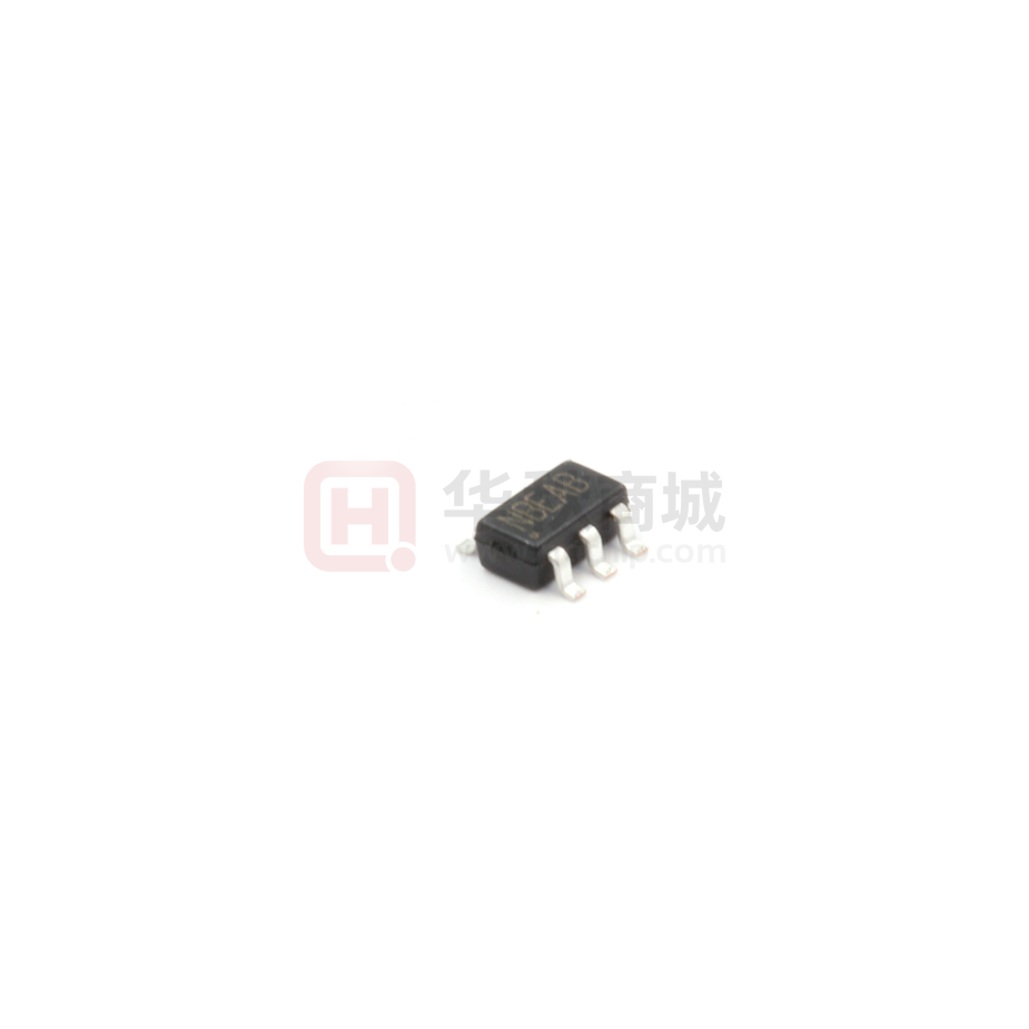
SOT23-5 Package
Applications
•
•
•
•
Cellular Handsets
Battery‐Powered Equipment
Wi-Fi Router
•
•
Hand‐Held Instruments
Portable Information Application
Adjustable power supply
General Description
The RY6050-ADJM5R is highly precise, low noise, positive voltage LDO regulators manufactured using CMOS
processes. The RY6050-ADJM5R achieves high ripple rejection and low dropout and consists of a standard voltage
source, an error correction, current limit, and a phase compensation circuit plus a driver transistor. External output
feedback, customers can easily get the required voltage. In order to make the load current does not exceed the current
capacity of the output transistor, built-in over-current protection, over temperature protection and short circuit
protection. The internal op amp with advanced structure, the output capacitor can be omitted. The RY6050ADJM5R is available in SOT23-5 package.
Typical Application Circuit
VIN
IN
VOUT
OUT
R1
CIN
1μF~10μF
ON/
OFF
EN
COUT
FB
GND
CFF
10μF
R2
Typical Application Circuit with FB
VOUT=0.8×(1+R1/R2)
Email: support@rychip.com
©RYCHIP Semiconductor Inc.
http://www.rychip.com
Page 1 / 9
�RY6050-ADJM5R
500mA Adjustable High-Speed Low Power LDO
Pin Description
Pin Configuration
TOP VIEW
VIN
1
GND
2
EN
3
5
OUT
4
FB
SOT23-5
Top Marking: 4bLL (device code: 4b, LL= lot number code)
Pin Description
Pin No.
Pin Name
Function
1
VIN
Input voltage pin for the regulator.
2
GND
Ground pin.
3
EN
Enable Control (Active high), Driving EN over 0.9 V turns on the regulator. Driving
EN below 0.4 V puts the regulator into shutdown mode.
4
FB
FB pin for adjustable output option.
5
OUT
Output voltage pin for the regulator.
Mark Rule
Mark
Part No.
Mode
Description
Package
T/R Qty
4bLL
70605021
RY6050-ADJM5R
RY6050-ADJM5R LDO, ADJ, 500mA,
SOT23-5
SOT23-5
3000PCS
Email: support@rychip.com
©RYCHIP Semiconductor Inc.
http://www.rychip.com
Page 2 / 9
�RY6050-ADJM5R
500mA Adjustable High-Speed Low Power LDO
Functional Block Diagram
IN
LSP
OUT
OTP
Enable
EN
FB
OCP
GND
Functional Block Diagram
Specifications
Absolute Maximum Ratings (1) (2)
Item
Min
Max
Unit
VIN voltage
2.0
8.0
V
1.0
3.3
V
VOUT voltage
Output Current
(3)
Power dissipation
600
(4)
Operating Ambient Temperature
Internally Limited
-40
Maximum junction temperature
Storage temperature, Tstg
Lead Temperature (Soldering, 10sec.)
mA
–50
85
°C
150
°C
85
°C
260
°C
Note (1): Exceeding these ratings may damage the device.
Note (2): The device is not guaranteed to function outside of its operating conditions.
Note (3): IOUT=PD/(VIN-VOUT)
Note (4): The maximum allowable power dissipation is a function of the maximum junction temperature, TJ(MAX),
the junction-to-ambient thermal resistance, RθJA, and the ambient temperature, TA. The maximum allowable power
dissipation at any ambient temperature is calculated using: PD (MAX) = (TJ(MAX) − TA)/RθJA. Exceeding the maximum
allowable power dissipation causes excessive die temperature, and the regulator goes into thermal shutdown.
Internal thermal shutdown circuitry protects the device from permanent damage. Thermal shutdown engages at
TJ=155°C (typical) and disengages at TJ= 140°C (typical).
Email: support@rychip.com
©RYCHIP Semiconductor Inc.
http://www.rychip.com
Page 3 / 9
�RY6050-ADJM5R
500mA Adjustable High-Speed Low Power LDO
Recommended Operating Conditions
Item
Min
Max
Unit
–40
125
°C
Operating temperature range
-40
85
°C
Input voltage VIN
2
6.5
V
Output current
0
500
mA
Operating junction temperature
(1)
Note (1): All limits specified at room temperature (TA = 25°C) unless otherwise specified. All room temperature
limits are 100% production tested. All limits at temperature extremes are ensured through correlation using standard
Statistical Quality Control (SQC) methods. All limits are used to calculate Average Outgoing Quality Level (AOQL).
Thermal Information
Item
Description
(1)(2)
Value
Unit
230
°C/W
RθJA
Junction-to-ambient thermal resistance
RθJC(top)
Junction-to-case (top) thermal resistance
152
°C/W
RθJB
Junction-to-board thermal resistance
56
°C/W
ψJT
Junction-to-top characterization parameter
31
°C/W
ψJB
Junction-to-board characterization parameter
55
°C/W
Note (1): The package thermal impedance is calculated in accordance to JESD 51-7.
Note (2): Thermal Resistances were simulated on a 4-layer, JEDEC board
Email: support@rychip.com
©RYCHIP Semiconductor Inc.
http://www.rychip.com
Page 4 / 9
�RY6050-ADJM5R
500mA Adjustable High-Speed Low Power LDO
Electrical Characteristics
TA = 25°C, unless otherwise noted.
Parameter
Symbol
Test Conditions
Min
Input Voltage
VIN
2
Feedback Voltage
VFB
784
Output Current
IOUT
VIN≥VOUT(S)+1.0V
Vdrop
Load Regulation
300mA
230
100mA
-40°C ≤ TJ
2.5V
≤125°C
300mA
70
250
100mA
430
300mA
700
∆𝑉𝑂𝑈𝑇
VOUT(S)+0.5 V≤VIN≤7V
∆𝑉𝐼𝑁 × 𝑉𝑂𝑈𝑇 IOUT=300mA
∆𝑉𝑂𝑈𝑇
VIN=VOUT(S)+1.0 V
𝑉𝑂𝑈𝑇
Supply Current
ISS1
VIN=VOUT(S)+1.0 V
Shutdown Current
Ishut
VIN=5V, VEN=0
Power Supply Rejection
Ratio
PSRR
VOUT=2.5V,
IOUT=20mA
f = 1KHz
Units
6.5
V
816
mV
VIN=VOUT(S)+1.0V,
ON/OFF Terminal is ON,
VOUT=0V
Ishort
EN “High Voltage
VENH
EN “Low” Voltage
VENL
EN “High Current
IENH
VIN=VEN=VOUT(T)+1V
EN “Low” Current
IENL
VIN=VOUT(T)+1V, VEN=VSS
Thermal Shutdown
Temperature
TSD
Thermal Shutdown
Hysteresis
ΔTSD
mA
mV
-
0.20
0.60
%/V
-
0.50
2
%
-
28
-
f = 10kHz
Short-circuit Current
Email: support@rychip.com
©RYCHIP Semiconductor Inc.
Max
500
60
1.2V
Line Regulations
800
100mA
3.3V
Dropout Voltage
VOUT=0.98VOUT (NOM)
Typ.
-
μA
0.1
μA
70
-
dB
50
-
dB
500
-
mA
1
V
0.5
V
-0.1
0.1
μA
-0.1
0.1
μA
155
°C
15
°C
ILOAD =10mA
http://www.rychip.com
Page 5 / 9
�RY6050-ADJM5R
500mA Adjustable High-Speed Low Power LDO
Typical Performance Characteristics (1)
Note (1): Typical performance characteristics below based on TA = 25°C, unless otherwise noted.
Load Regulation
Load Regulation
Load Regulation
VOUT=3.3V
VOUT= 2.5V
VOUT=1.2V
Line Regulation
Line Regulation
Line Regulation
VOUT=3.3V
VOUT=2.5V
VOUT=1.2V
Power Supply Rejection Ration
Power Supply Rejection Ration
Power Supply Rejection Ration
VIN=3.3V, VOUT=1.2V, IOUT=20mA
VIN=3.3V, VOUT=2.5V, IOUT=20mA
VIN=5V, VOUT=3.3V, IOUT=20mA
Vin Start Up
EN Start Up
VIN=3.3V, VOUT=2.5V, IOUT=1mA
VIN=3.3V, VOUT=2.5V, IOUT=1mA
Steady State
VIN=3.3V, VOUT=2.5V, IOUT=350mA
Email: support@rychip.com
©RYCHIP Semiconductor Inc.
http://www.rychip.com
Page 6 / 9
�RY6050-ADJM5R
500mA Adjustable High-Speed Low Power LDO
Applications Information
Setting the Output Voltage
RY6050-ADJM5R require an input capacitor and an output capacitor. These components are critical to the
performance of the device. The output voltage can be programmed by resistor divider.
𝑉𝑂𝑈𝑇 = 𝑉𝐹𝐵 ×
𝑅1 + 𝑅2
𝑅2
VOUT(V)
R1(KΩ)
R2(KΩ)
CIN(μF)
COUT(μF)
CFF
1
25.00
100
1~10
10
Opt.
1.05
31.25
100
1~10
10
Opt.
1.2
50.00
100
1~10
10
Opt.
1.5
87.50
100
1~10
10
Opt.
1.8
125.00
100
1~10
10
Opt.
2.5
212.50
100
1~10
10
Opt.
2.8
250.00
100
1~10
10
Opt.
3.3
312.50
100
1~10
10
Opt.
Low ESR Capacitors
With the RY6050-ADJM5R, a stable output voltage is achievable even if used with low ESR capacitors as a phase
compensation circuit is built-in. In order to ensure the effectiveness of the phase compensation, we suggest that an
output capacitor (COUT) is connected as close as possible to the output pin (VOUT) and the GND pin. Please use an
output capacitor with a capacitance value of 10uF. Also, please connect an input capacitor (CIN) of 10uF between
the VIN pin and the GND pin in order to ensure a stable power input. Stable phase compensation may not be ensured
if the capacitor runs out capacitance when depending on bias and temperature. In case the capacitor depends on the
bias and temperature, please make sure the capacitor can ensure the actual capacitance.
Current Limiter, Short-Circuit Protection
The RY6050-ADJM5R includes a combination of a fixed current limiter circuit & a feedback circuit, which aid the
operations of the current limiter and circuit protection. When the load current reaches the current limit level, the
fixed current limiter circuit operates and output voltage drops. As a result of this drop-in output voltage, the feedback
circuit operates, output voltage drops further and output current decreases.
EN pin
The IC's internal circuitry can be shutdown via the signal from the EN pin with the RY6050-ADJM5R. Driving EN
over 1 V turns on the regulator. Driving EN below 0.5 V puts the regulator into shutdown mode. The operational
logic of the IC's EN pin is selectable. Note that as the standard RY6050-ADJM5R type's regulator is 'High Active/No
Pull-Down', operations will become unstable with the EN pin open. Although the EN pin is equal to an inverter
input with CMOS hysteresis, with either the pull-up or pull-down options, the EN pin input current will increase
when the IC is in operation. We suggest that you use this IC with either a VIN voltage or a GND voltage input at the
EN pin. If this IC is used with the correct specifications for the EN pin, the operational logic is fixed and the IC will
Email: support@rychip.com
©RYCHIP Semiconductor Inc.
http://www.rychip.com
Page 7 / 9
�RY6050-ADJM5R
500mA Adjustable High-Speed Low Power LDO
operate normally. However, supply current may increase as a result of through current in the IC's internal circuitry.
Notes on Use
1. Please use this IC within the stated absolute maximum ratings. The IC is liable to malfunction should the ratings
be exceeded.
2. Where wiring impedance is high, operations may become unstable due to noise and/or phase lag depending on
output current. Please keep the resistance low between VIN and GND wiring.
3. Please wire the input capacitor (CIN) and the output capacitor (COUT) as close to the IC as possible.
Email: support@rychip.com
©RYCHIP Semiconductor Inc.
http://www.rychip.com
Page 8 / 9
�RY6050-ADJM5R
500mA Adjustable High-Speed Low Power LDO
Packaging Information
5-Pin SOT23 Packaging Information
SOT23-5
2.80
3.00
0.95
BSC
0.60
TYP
1.20
TYP
1.50
2.60
1.70
3.00
2.60
TYP
PIN 1
TOP VIEW
RECOMMENDED PAD LAYOUT
GAUGE PLANE
0.25 BSC
0.90
1. 30
1.45 MAX
SEATING PLANE
0.30
0.50
0.95 BSC
FRONT VIEW
0.00
0.15
0°~8°
0.30
0.55
0.09
0.20
SIDE VIEW
NOTE:
1. CONTRO L DI MENSION IS IN INCHES. DIMENSION I N BRACKET IS IN MILLIMETERS.
2. PACKAG E LENGTH DOES NOT INCLUDE MOLD FLASH, PROTRUSIONS OR GATE BURRS.
3. PACKAG E WIDTH DO ES NOT INCLUDE I NTERLEAD FLASH OR PROTRUSIONS.
4. LEAD COPLANARITY (BO TTO M O F LEADS AFTER FORMING) SHALL BE 0. 004" INCHES MAX.
5. DRAWING CONFORMS TO JEDEC MS-012, VARIATION BA.
6. DRAWING IS NOT TO SCALE.
Email: support@rychip.com
©RYCHIP Semiconductor Inc.
http://www.rychip.com
Page 9 / 9
�