RY3715
18V Output 1.2MHz Boost Regulator
Features
•
•
•
•
•
•
•
•
•
•
•
•
•
2.3V to 5.5V Input Voltage
Up to 18V Output Voltage
Integrated 60mΩ Power MOSFET
1.2MHz Fixed Switching Frequency
Internal 4A Switch Current Limit
Power Save Operation Mode at Light Load
Internal 1.5mS Soft Start Time
•
Up to 85% Efficiency@3.6V Input 12V Output
Output Short Circuit Protection
Output Over-Voltage Protection
Thermal Shutdown Protection
Output Adjustable from 0.6V
-40°C to +85°C Temperature Range
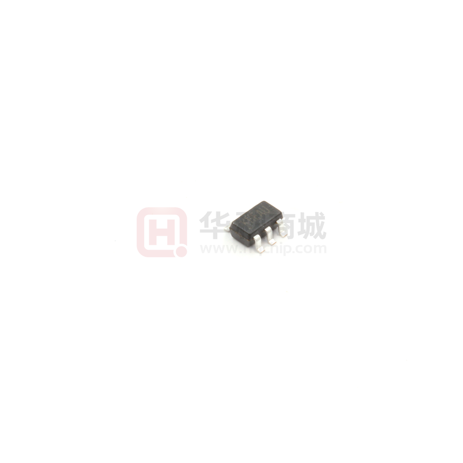
Available in SOT23-6 Package
Applications
•
•
•
Wearable Devices
Sensor Power Supply
•
Battery-Powered Equipment
Portable Medical Equipment
General Description
The RY3715 is a highly integrated boost converter designed for applications requiring high voltage and high
efficiency solution. The RY3715 integrates a 20V power switch, it can output up to 18V from input of a Li+ battery
or two cell alkaline batteries in series.
The RY3715 operates with a switching frequency at 1.2MHz. This allows the use of small external components.
RY3715 has typical 4A switch current limit. It has 1.5mS built-in soft start time to minimize the inrush current. The
RY3715 also implements output short circuit protection, output over-voltage protection and thermal shutdown.
The RY3715 is available in a small SOT23-6 package.
Typical Application Circuit
ON/
OFF
R1
100k 1%
EN
FB
VIN
C1
22μF/25V
Ceramic
IN
GND
NC
SW
R2
3.48k 1%
C2
22μF/25V
Ceramic
L1 4.7μH
VOUT18V
D1
Typical Application Circuit
Email: support@rychip.com
©RYCHIP Semiconductor Inc.
http://www.rychip.com
Page 1 / 11
�RY3715
18V Output 1.2MHz Boost Regulator
Package and Pin Description
Pin Configuration
TOP VIEW
SW
1
6
NC
GND
2
5
IN
FB
3
4
EN
SOT23-6
Top Marking: KHYLL (device code: KH, Y=year code, LL= lot number code)
Pin Description
Pin
Name
Function
1
SW
Power Switch Output. SW is the drain of the internal MOSFET switch. Connect the
power inductor and output rectifier to SW
2
GND
3
FB
Feedback Input. The FB voltage is 0.6V. Connect a resistor divider to FB
4
EN
Regulator On/Off Control Input. A high input at EN turns on the converter, and a
low input turns it off. When not used, connect EN to the input supply for automatic
startup
5
IN
Input Supply Pin
6
NC
Not Connection
Ground Pin
Order Information (1)
Marking
Part No.
Model
Description
Package
T/R Qty
KHYLL
70390013
RY3715
RY3715 Boost, VIN 2.3-5.5V, VOUT VIN18V, 1.2MHz, VFB 0.6V, SOT23-6
SOT23-6
3000PCS
Note (1): All RYCHIP parts are Pb-Free and adhere to the RoHS directive.
Email: support@rychip.com
©RYCHIP Semiconductor Inc.
http://www.rychip.com
Page 2 / 11
�RY3715
18V Output 1.2MHz Boost Regulator
Specifications
Absolute Maximum Ratings (1) (2)
Item
Min
Max
Unit
VIN EN voltage
-0.3
6
V
SW voltage
-0.3
19
V
–0.3
6
V
All Other Pins
Power dissipation
(3)
Internally Limited
Operating junction temperature, TJ
-40
150
°C
Storage temperature, Tstg
–65
150
°C
260
°C
Lead Temperature (Soldering, 10sec.)
Note (1): Exceeding these ratings may damage the device.
Note (2): The device is not guaranteed to function outside of its operating conditions.
Note (3): The maximum allowable power dissipation is a function of the maximum junction temperature, TJ(MAX),
the junction-to-ambient thermal resistance, RθJA, and the ambient temperature, TA. The maximum allowable power
dissipation at any ambient temperature is calculated using: PD (MAX) = (TJ(MAX) − TA)/RθJA. Exceeding the maximum
allowable power dissipation causes excessive die temperature, and the regulator goes into thermal shutdown.
Internal thermal shutdown circuitry protects the device from permanent damage. Thermal shutdown engages at
TJ=160°C (typical) and disengages at TJ= 130°C (typical).
ESD Ratings
Item
Description
Value
Unit
V(ESD-HBM)
Human Body Model (HBM)
ANSI/ESDA/JEDEC JS-001-2014
Classification, Class: 2
±2000
V
V(ESD-CDM)
Charged Device Mode (CDM)
ANSI/ESDA/JEDEC JS-002-2014
Classification, Class: C0b
±200
V
ILATCH-UP
JEDEC STANDARD NO.78E APRIL 2016
Temperature Classification,
Class: I
±150
mA
Min
Max
Unit
–40
125
°C
Operating temperature range
-40
85
°C
Input voltage VIN
2.3
5.5
V
18
V
1
A
Recommended Operating Conditions
Item
Operating junction temperature
(1)
Output voltage VOUT
Typical Output Current IOUT
0
Note (1): All limits specified at room temperature (TA = 25°C) unless otherwise specified. All room temperature
limits are 100% production tested. All limits at temperature extremes are ensured through correlation using standard
Statistical Quality Control (SQC) methods. All limits are used to calculate Average Outgoing Quality Level (AOQL).
Email: support@rychip.com
©RYCHIP Semiconductor Inc.
http://www.rychip.com
Page 3 / 11
�RY3715
18V Output 1.2MHz Boost Regulator
Thermal Information
Item
Description
(1)(2)
Value
Unit
105
°C/W
RθJA
Junction-to-ambient thermal resistance
RθJC(top)
Junction-to-case (top) thermal resistance
55
°C/W
RθJB
Junction-to-board thermal resistance
17.5
°C/W
ψJT
Junction-to-top characterization parameter
3.5
°C/W
ψJB
Junction-to-board characterization parameter
17.5
°C/W
Note (1): The package thermal impedance is calculated in accordance to JESD 51-7.
Note (2): Thermal Resistances were simulated on a 4-layer, JEDEC board
Electrical Characteristics (1) (2)
VIN=5V, TA=25°C, unless otherwise specified.
Parameter
Test Conditions
Input voltage range
Min
Typ.
2.3
Output voltage range
Max
Unit
5.5
V
18
V
Supply Current (Quiescent)
VFB =110%
150
200
µA
Supply Current (Shutdown)
VEN =0 or EN = GND
0.1
1
µA
600
612
mV
60
120
mΩ
Feedback Voltage
588
SW On Resistance
Current Limit
4
A
Output Over Voltage Protection
Threshold
19
V
Output Over voltage protection
hysteresis
800
mV
Switching Frequency
1.2
MHz
90
%
100
nS
Maximum Duty Cycle
Duty cycle=50%
VFB=90%
Minimum On-Time
EN Rising Threshold
1.2
V
EN Falling Threshold
0.8
EN Threshold Hysteresis
100
Wake up VIN Voltage
Under-Voltage Lockout Threshold
Shutdown VIN Voltage
2.0
mV
2.2
V
1.8
V
200
mV
Soft Start
1.5
mS
Thermal Shutdown
160
℃
Thermal Hysteresis
30
℃
Hysteresis VIN voltage
1.6
V
Note (1): MOSFET on-resistance specifications are guaranteed by correlation to wafer level measurements.
Note (2): Thermal shutdown specifications are guaranteed by correlation to the design and characteristics analysis.
Email: support@rychip.com
©RYCHIP Semiconductor Inc.
http://www.rychip.com
Page 4 / 11
�RY3715
18V Output 1.2MHz Boost Regulator
Typical Performance Characteristics (1) (2)
Note (1): Performance waveforms are tested on the evaluation board.
Note (2): VIN =5V, VOUT=12V, TA = +25ºC, unless otherwise noted.
Efficiency vs. Load Current
Load Regulation
Line Regulation
VOUT=12V
VOUT=12V
VOUT=12V
Output Ripple Voltage
Output Ripple Voltage
Output Ripple Voltage
VIN=5V, VOUT=12V, IOUT=0A
VIN=5V, VOUT=12V, IOUT=200mA
VIN=5V, VOUT=12V, IOUT=400mA
Enable Startup at No Load
Enable Shutdown at No Load
Enable Startup at Heavy Load
VIN=5V, VOUT=12V
VIN=5V, VOUT=12V
VIN=5V, VOUT=12V, IOUT=400mA
Enable Shutdown at Heavy Load
Power Up at No Load
Power Up at Heavy Load
VIN=5V, VOUT=12V, IOUT=400mA
VIN=5V, VOUT=12V, IOUT=0A
VIN=5V, VOUT=12V, IOUT=400mA
Email: support@rychip.com
©RYCHIP Semiconductor Inc.
http://www.rychip.com
Page 5 / 11
�RY3715
18V Output 1.2MHz Boost Regulator
Functional Block Diagram
Block Diagram
Functions Description
Under-Voltage Lockout (UVLO)
Under-voltage lockout (UVLO) protects the chip from operating at an insufficient supply voltage. UVLO protection
monitors the internal regulator voltage. When the voltage is lower than UVLO threshold voltage, the device is shut
off. When the voltage is higher than UVLO threshold voltage, the device is enabled again.
Enable and Disable
When the input voltage is above maximal UVLO rising threshold and the EN pin is pulled high, the RY3715 is
enabled. When the EN pin is pulled low, the RY3715 goes into shutdown mode. In shutdown mode, less than 1μA
input current is consumed.
Soft-Start
The RY3715 begins soft start when the EN pin is pulled high. at the beginning of the soft start period, the isolation
FET is turned on slowly to charge the output capacitor. After the pre-charge phase, the RY3715 starts switching.
This is called switching soft start phase. An internal soft start circuit limits the peak inductor current according to
the output voltage. The switching soft start phase is about 1.5ms typically. The soft start function reduces the inrush
current during startup.
Over-Voltage Protection
The RY3715 has internal output over-voltage protection (OVP) function. When the output voltage exceeds the
Email: support@rychip.com
©RYCHIP Semiconductor Inc.
http://www.rychip.com
Page 6 / 11
�RY3715
18V Output 1.2MHz Boost Regulator
OVP threshold, the device stops switching. Once the output voltage falls 800mV below the OVP threshold, the
device resumes operation again.
Output Short Circuit Protection
When the VOUT pin is shorted to ground, the RY3715 stop switching. This function protects the device from being
damaged when the output is shorted to ground.
Thermal Shutdown
Thermal shutdown prevents the chip from operating at exceedingly high temperatures. When the silicon die
temperature exceeds 160°C, it shuts down the whole chip. When the temperature falls below its lower threshold
(Typ. 130°C) the chip is enabled again.
PWM Mode
The RY3715 uses a quasi-constant 1.2MHz frequency pulse width modulation (PWM) at moderate to heavy load
current. Based on the input voltage to output voltage ratio, a circuit predicts the required off-time. At the beginning
of the switching cycle, the NMOS switching FET, shown in the functional block diagram, is turned on. The input
voltage is applied across the inductor and the inductor current ramps up. In this phase, the output capacitor is
discharged by the load current. When the inductor current hits the current threshold that is set by the output of the
error amplifier, the PWM switch is turned off, and the power diode is forward-biased. The inductor transfers its
stored energy to replenish the output capacitor and supply the load. When the off-time is expired, the next switching
cycle starts again. The error amplifier compares the FB pin voltage with an internal reference voltage, and its output
determines the inductor peak current.
The RY3715 has a built-in compensation circuit that can accommodate a wide range of input voltage, output voltage,
inductor value and output capacitor value for stable operation.
Power Save Mode
The RY3715 integrates a power save mode with pulse frequency modulation (PFM) to improve efficiency at light
load. When the load current decreases, the inductor peak current set by the output of the error amplifier declines to
regulate the output voltage. When the FB voltage hits the PFM reference voltage, the RY3715 goes into the power
save mode. In the power save mode, when the FB voltage rises and hits the PFM reference voltage, the device
continuous switching for several cycles because of the delay time of the internal comparator. Then it stops switching.
The load is supplied by the output capacitor and the output voltage declines. When the FB voltage falls below the
PFM reference voltage, after the delay time of the comparator, the device starts switching again to ramp up the
output voltage.
Email: support@rychip.com
©RYCHIP Semiconductor Inc.
http://www.rychip.com
Page 7 / 11
�RY3715
18V Output 1.2MHz Boost Regulator
Applications Information
Setting the Output Voltage
RY3715 are internally compensated and do not require external components to achieve stable operation. The output
voltage can be programmed by resistor divider, as shown in Equation 𝑉𝑂𝑈𝑇 = 𝑉𝐹𝐵 ×
𝑅1+𝑅2
𝑅2
.
VOUT
R1
COUT
VFE EDB AC K
R2
Inductor Selection
Because the selection of the inductor affects steady state operation, transient behavior, and loop stability, the inductor
is the most important component in power regulator design. There are three important inductor specifications,
inductor value, saturation current, and dc resistance (DCR).
The RY3715 is designed to work with inductor values between 2.2μH and 22μH. Follow the Equation below to
calculate the inductor’s peak current for the application. To calculate the current in the worst case, use the minimum
input voltage, maximum output voltage, and maximum load current of the application. To have enough design
margin, choose the inductor value with -30% tolerance, and a low power-conversion efficiency for the calculation.
In a boost regulator, the inductor dc current can be calculated with Equation:
𝐼𝐿(𝐷𝐶) =
𝑉𝑂𝑈𝑇 × 𝐼𝑂𝑈𝑇
𝑉𝐼𝑁 × 𝜂
Where
• VOUT = output voltage
• IOUT = output current
• VIN = input voltage
• η = power conversion efficiency, use 80% for most applications
The inductor ripple current is calculated with the Equation 3 for an asynchronous boost converter in continuous
conduction mode (CCM).
𝛥𝐼𝐿(𝑃−𝑃) =
𝑉𝐼𝑁 × (𝑉𝑂𝑈𝑇 + 𝑉𝐷𝐼𝑂𝐷𝐸 − 𝑉𝐼𝑁 )
𝐿 × 𝐹𝑆 × (𝑉𝑂𝑈𝑇 + 𝑉𝐷𝐼𝑂𝐷𝐸 )
Where
•
•
ΔIL(P-P) = inductor ripple current
L = inductor value
Email: support@rychip.com
©RYCHIP Semiconductor Inc.
http://www.rychip.com
Page 8 / 11
�RY3715
18V Output 1.2MHz Boost Regulator
• VIN = input voltage
• VOUT = output voltage
• VDIODE = output diode forward voltage
• FS = switching frequency, Hertz
Therefore, the inductor peak current is calculated with Equation:
𝐼𝐿(𝑃) = 𝐼𝐿(𝐷𝐶) +
𝛥𝐼𝐿(𝑃−𝑃)
2
Normally, it is advisable to work with an inductor peak-to-peak current of less than 40% of the average inductor
current for maximum output current. A smaller ripple from a larger valued inductor reduces the magnetic hysteresis
losses in the inductor and EMI. Bit in the same way, load transient response time is increased.
Because the RY3715 is for relatively small output current application, the inductor peak-to-peak current could be
as high as 200% of the average current with a small inductor value, which means the RY3715 always works in DCM
mode.
Input and Output Capacitor Selection
The output capacitor is mainly selected to meet the requirements for output ripple and loop stability. This ripple
voltage is related to the capacitor’s capacitance and its equivalent series resistance (ESR). Assuming a ceramic
capacitor with zero ESR, the minimum capacitance needed for a given ripple can be calculated by:
𝐶𝑂𝑈𝑇 =
𝐼𝑂𝑈𝑇 × 𝐷𝑀𝐴𝑋
𝐹𝑆 × 𝑉𝑅𝐼𝑃𝑃𝐿𝐸
Where
• DMAX = maximum switching duty cycle
• IRIPPLE = peak to peak output voltage ripple
The ESR impact on the output ripple must be considered if tantalum or aluminum electrolytic capacitors are used.
Care must be taken when evaluating a ceramic capacitor’s derating under dc bias, aging, and ac signal. For example,
the dc bias can significantly reduce capacitance. A ceramic capacitor can lose more than 50% of its capacitance at
its rated voltage. Therefore, always leave margin on the voltage rating to ensure adequate capacitance at the required
output voltage.
It is recommended to use the output capacitor with effective capacitance in the range of 10μF to 22μF. The output
capacitor affects the small signal control loop stability of the boost regulator. If the output capacitor is below the
range, the boost regulator can potentially become unstable. Increasing the output capacitor makes the output voltage
ripple smaller in PWM mode.
For input capacitor, a ceramic capacitor with more than 1.0μF is enough for most applications.
Diode Selection
A Schottky diode should be used for the output diode. The forward current rating of the diode should be higher than
the load current, and the reverse voltage rating must be higher than the output voltage. Do not use ordinary rectifier
diodes, since slow switching speeds and long recovery times cause the efficiency and the load regulation to suffer.
Email: support@rychip.com
©RYCHIP Semiconductor Inc.
http://www.rychip.com
Page 9 / 11
�RY3715
18V Output 1.2MHz Boost Regulator
Layout Guidelines
PC board layout is an important part of DC-DC converter design. Poor board layout can disrupt the performance of
a DC-DC converter and surrounding circuitry by contributing to EMI, ground bounce, and resistive voltage loss in
the traces. These can send erroneous signals to the DC-DC converter resulting in poor regulation or instability. Good
layout can be implemented by following a few simple design rules.
1. Minimize area of switched current loops. In a buck regulator there are two loops where currents are switched
rapidly. The first loop starts from the CIN input capacitor, to the regulator VIN terminal, to the regulator SW
terminal, to the inductor then out to the output capacitor COUT and load. The second loop starts from the output
capacitor ground, to the regulator GND terminals, to the inductor and then out to COUT and the load. To
minimize both loop areas the input capacitor should be placed as close as possible to the VIN terminal.
Grounding for both the input and output capacitors should consist of a small localized topside plane that
connects to GND. The inductor should be placed as close as possible to the SW pin and output capacitor.
2. Minimize the copper area of the switch node. The SW terminals should be directly connected with a trace that
runs on top side directly to the inductor. To minimize IR losses this trace should be as short as possible and with
an enough width. However, a trace that is wider than 100 mils will increase the copper area and cause too much
capacitive loading on the SW terminal. The inductors should be placed as close as possible to the SW terminals
to further minimize the copper area of the switch node.
3. Have a single point ground for all device analog grounds. The ground connections for the feedback components
should be connected then routed to the GND pin of the device. This prevents any switched or load currents from
flowing in the analog ground plane. If not properly handled, poor grounding can result in degraded load
regulation or erratic switching behavior.
4. Minimize trace length to the FB terminal. The feedback trace should be routed away from the SW pin and
inductor to avoid contaminating the feedback signal with switch noise.
5. Make input and output bus connections as wide as possible. This reduces any voltage drops on the input or
output of the converter and can improve efficiency. If voltage accuracy at the load is important make sure
feedback voltage sense is made at the load. Doing so will correct for voltage drops at the load and provide the
best output accuracy.
Top Layer
Bottom Layer
Sample Board Layout
Email: support@rychip.com
©RYCHIP Semiconductor Inc.
http://www.rychip.com
Page 10 / 11
�RY3715
18V Output 1.2MHz Boost Regulator
Package Description
SOT23-6
2.80
3.00
0.95
BSC
0.60
TYP
1.20
TYP
EXAMPLE
TOP MARK
AAAAA
1.50
2.60
1.70
3.00
2.60
TYP
PIN 1
TOP VIEW
RECOMMENDED PAD LAYOUT
GAUGE PLANE
0.25 BSC
0.90
1. 30
1.45 MAX
SEATING PLANE
0.30
0.50
0.95 BSC
FRONT VIEW
0.00
0.15
0°~8°
0.30
0.55
0.09
0.20
SIDE VIEW
NOTE:
1. CONTRO L DI MENSION IS IN INCHES. DIMENSION I N BRACKET IS IN MILLIMETERS.
2. PACKAG E LENGTH DOES NOT INCLUDE MOLD FLASH, PROTRUSIONS OR GATE BURRS.
3. PACKAG E WIDTH DO ES NOT INCLUDE I NTERLEAD FLASH OR PROTRUSIONS.
4. LEAD COPLANARITY (BO TTO M O F LEADS AFTER FORMING) SHALL BE 0. 004" INCHES MAX.
5. DRAWING CONFORMS TO JEDEC MS-012, VARIATION BA.
6. DRAWING IS NOT TO SCALE.
Email: support@rychip.com
©RYCHIP Semiconductor Inc.
http://www.rychip.com
Page 11 / 11
�