ESD5471S
ESD5471S
1-Line, Bi-directional, Transient Voltage Suppressor
http//:www.sh-willsemi.com
Descriptions
The ESD5471S is a bi-directional TVS (Transient Voltage
Suppressor). It is specifically designed to protect sensitive
electronic components which are connected to low speed
data lines and control lines from over-stress caused by ESD
(Electrostatic Discharge), EFT (Electrical Fast Transients)
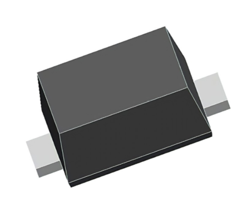
SOD-523 (Top View)
and Lightning.
The ESD5471S may be used to provide ESD protection up to
±30kV
(contact
and
air
discharge)
according
to
IEC61000-4-2, and withstand peak pulse current up to 6A
(8/20μs) according to IEC61000-4-5.
Pin1
Pin2
The ESD5471S is available in SOD-523 package. Standard
products are Pb-free and Halogen-free.
Circuit diagram
Features
Reverse stand-off voltage: ±5V Max
Transient protection for each line according to
Pin1
TA *
Pin2
IEC61000-4-2 (ESD): ±30kV (contact and air discharge)
IEC61000-4-4 (EFT): 40A (5/50ns)
IEC61000-4-5 (surge): 6A (8/20μs)
TA = Device code
Capacitance: CJ = 9pF typ.
Low leakage current
Low clamping voltage: VCL = 12V typ. @ IPP = 16A (TLP)
Solid-state silicon technology
*
Cellular handsets
Tablets
Laptops
Other portable devices
Network communication devices
Will Semiconductor Ltd.
Marking (Top View)
Order information
Applications
= Month code ( A~Z)
Device
Package
Shipping
ESD5471S-2/TR SOD-523 3000/Tape&Reel
1
Revision 1.5, 2021/09/24
�ESD5471S
Absolute maximum ratings
Parameter
Symbol
Rating
Unit
Peak pulse power (tp = 8/20μs)
Ppk
72
W
Peak pulse current (tp = 8/20μs)
IPP
6
A
ESD according to IEC61000-4-2 air discharge
VESD
ESD according to IEC61000-4-2 contact discharge
±30
kV
±30
TJ
125
oC
Operating temperature
TOP
-40~85
oC
Lead temperature
TL
260
oC
TSTG
-55~150
oC
Junction temperature
Storage temperature
Electrical characteristics (TA=25 oC, unless otherwise noted)
I
VRWM Reverse stand-off voltage
IR
Reverse leakage current
VCL
Clamping voltage
IPP
Peak pulse current
IPP
IHOLD
VCL
VTRIG VHOLD
VBR VRWM
IBR
ITRIG
IR
IR
ITRIG
IBR
VRWM VBR
VHOLD VTRIG
VCL
V
IHOLD
VTRIG Reverse trigger voltage
ITRIG
Reverse trigger current
VBR
Reverse breakdown voltage
IBR
Reverse breakdown current
VHOLD Reverse holding voltage
IPP
IHOLD
Reverse holding current
Definitions of electrical characteristics
Will Semiconductor Ltd.
2
Revision 1.5, 2021/09/24
�ESD5471S
Electrical characteristics (TA=25 oC, unless otherwise noted)
Parameter
Symbol
Condition
Min.
Typ.
Max.
Unit
±5
V
1
μA
Reverse stand-off voltage
VRWM
Reverse leakage current
IR
VRWM = 5V
VBR
IBR = 1mA
5.1
V
IHOLD = 50mA
5.1
V
Reverse breakdown voltage
Reverse holding voltage
VHOLD
Clamping voltage 1)
VCL
IPP = 16A, tp = 100ns
12
V
Clamping voltage 2)
VCL
VESD = 8kV
12
V
Clamping voltage 3)
VCL
Dynamic resistance 1)
RDYN
Junction capacitance
CJ
IPP = 1A, tp = 8/20μs
8
V
IPP = 6A, tp = 8/20μs
12
V
Ω
0.28
VR = 0V, f = 1MHz
9
12
pF
VR = 5V, f = 1MHz
6
8
pF
Notes:
1) TLP parameter: Z0 = 50Ω , tp = 100ns, tr = 2ns, averaging window from 60ns to 80ns. RDYN is calculated from 4A to
16A.
2)
Contact discharge mode, according to IEC61000-4-2.
3)
Non-repetitive current pulse, according to IEC61000-4-5.
Will Semiconductor Ltd.
3
Revision 1.5, 2021/09/24
�ESD5471S
Typical characteristics (TA=25oC, unless otherwise noted)
Time to half-value: T2= 20s
Current (%)
Peak pulse current (%)
100
90
Front time: T1= 1.25 T = 8s
100
90
50
T2
10
10
0
0
tr = 0.7~1ns
Time (s)
T1
10
11
10
CJ - Junction capacitance (pF)
Pulse waveform: tp = 8/20s
VC - Clamping voltage (V)
Time (ns)
Contact discharge current waveform per IEC61000-4-2
8/20μs waveform per IEC61000-4-5
Pin1 to Pin2
Pin2 to Pin1
9
8
7
6
t
60ns
30ns
20
T
0
1
2
3
4
5
6
f = 1MHz
VAC = 50mV
9
8
7
6
5
-5
7
-4
-3
-2
-1
0
1
2
3
IPP - Peak pulse current (A)
VR - Reverse voltage (V)
Clamping voltage vs. Peak pulse current
Capacitance vs. Reverse voltage
4
5
1000
Peak pulse power (W)
100
% of Rated power
100
10
1
1
10
100
Pulse time (s)
60
40
20
0
1000
0
25
50
75
100
125
150
o
TA - Ambient temperature ( C)
Non-repetitive peak pulse power vs. Pulse time
Will Semiconductor Ltd.
80
Power derating vs. Ambient temperature
4
Revision 1.5, 2021/09/24
�ESD5471S
Typical characteristics (TA=25oC, unless otherwise noted)
ESD clamping
ESD clamping
(+8kV contact discharge per IEC61000-4-2)
(-8kV contact discharge per IEC61000-4-2)
20
16
TLP current (A)
12
8
4
0
-4
-8
Z0 = 50
-12
tr = 2ns
-16
tp = 100ns
-20
-14 -12 -10 -8 -6 -4 -2 0
2
4
6
8 10 12 14
TLP voltage (V)
TLP Measurement
Will Semiconductor Ltd.
5
Revision 1.5, 2021/09/24
�ESD5471S
PACKAGE OUTLINE DIMENSIONS
SOD-523
A1
E
b
D
E2
E1
A
TOP VIEW
SIDE VIEW
0.4
c
2
1.5
1
0.5
SIDE VIEW
Symbol
θ
RECOMMENDED LAND PATTERN(Unit:mm)
Dimensions in Millimeters
Min.
Typ.
Max.
A
0.51
-
0.77
A1
0.50
0.60
0.70
b
0.25
-
0.40
c
0.08
-
0.15
D
0.75
0.80
0.85
E
1.10
1.20
1.30
E1
1.50
1.60
1.70
E2
0.20 Ref.
θ
7︒C Ref.
Will Semiconductor Ltd.
6
Revision 1.5,2021/09/24
�ESD5471S
TAPE AND REEL INFORMATION
Reel Dimensions
RD
Reel Dimensions
Tape Dimensions
W
P1
Quadrant Assignments For PIN1 Orientation In Tape
Q1
Q2
Q1
Q2
Q3
Q4
Q3
Q4
RD
Reel Dimension
W
Overall width of the carrier tape
P1
Pitch between successive cavity centers
Pin1
Pin1 Quadrant
Will Semiconductor Ltd.
User Direction of Feed
7inch
13inch
1 8mm
12mm
16mm
2mm
4mm
8mm
Q1
Q2
Q3
7
Q4
Revision 1.5,2021/09/24
�
很抱歉,暂时无法提供与“ESD5471S-2/TR”相匹配的价格&库存,您可以联系我们找货
免费人工找货- 国内价格
- 50+0.11700
- 500+0.10575
- 5000+0.09825
- 10000+0.09450
- 30000+0.09075
- 50000+0.08850
- 国内价格
- 20+0.20423
- 200+0.16168
- 600+0.13803