May. 2022
S C B 3 3 S 1 2 8 3 20 A E
SCB33S128160AE
SCB33S128800AE
128 M b it Sy n c h r o n o u s DRAM
EU Ro H S Co m p li a n t Pr o d u c t s
D a t a She e t
Re v . F
�Data Sheet
SCB33S128[32/16/80]0AE
128Mbit Synchronous DRAM
Revision History
Date
Version
Subjects(major changes since last revision)
2016-07
A
Initial Release
2016-09
B
Add the “I” , “A2” and “X” grade component
2016-11
C
Update the “I” grade temperature and IDD specification
2017-03
D
Redefine the operating temperature
2018-02
E
Add timing diagram and IDD test condition
Format review (2020-05)
2022-05
F
Add Remark(P7)
We Listen to Your Comments
Any information within this document that you feel is wrong, unclear or missing at all? Your feedback will help us to
continuously improve the quality of this document. Please send your proposal (including a reference to this document) to:
info@unisemicon.com
UniIC_Techdoc, Rev. F 2022-05
2 / 52
�Data Sheet
SCB33S128[32/16/80]0AE
128Mbit Synchronous DRAM
Contents
Contents .................................................................................................................................................................................... 3
1
2
Overview ........................................................................................................................................................................... 4
1.1
Features ............................................................................................................................................................... 4
1.2
Description ........................................................................................................................................................... 5
Configuration ..................................................................................................................................................................... 7
2.1
3
4
Pin Description ..................................................................................................................................................... 7
Functional Description ..................................................................................................................................................... 12
3.1
Operation Definition ............................................................................................................................................ 12
3.2
Initialization......................................................................................................................................................... 13
3.3
Mode Register Definition .................................................................................................................................... 13
3.4
Burst Type .......................................................................................................................................................... 14
3.5
Commands ......................................................................................................................................................... 15
3.6
Operations .......................................................................................................................................................... 16
Electrical Characteristics ................................................................................................................................................. 17
4.1
Operating Conditions .......................................................................................................................................... 17
4.2
AC Characteristics .............................................................................................................................................. 20
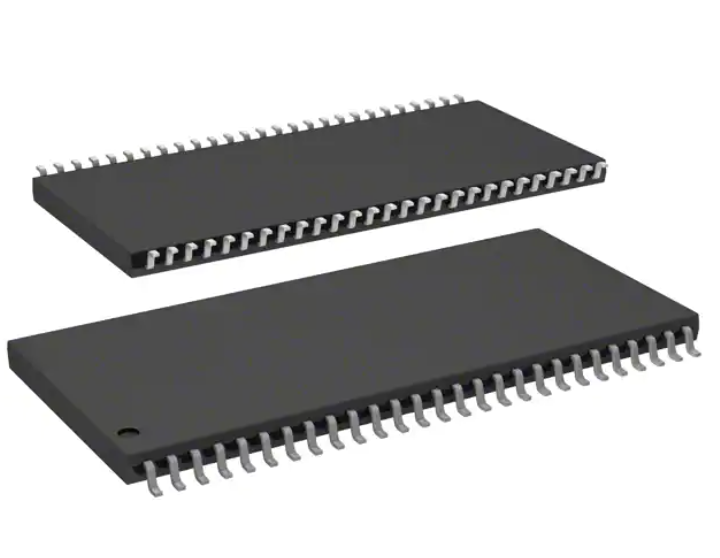
5
Package Outlines ............................................................................................................................................................ 22
6
Product Nomenclature..................................................................................................................................................... 26
7
Timing Diagram and IDD Test Condition ......................................................................................................................... 27
7.1
Initialization......................................................................................................................................................... 27
7.2
Auto-refresh and Self-refresh ............................................................................................................................. 28
7.3
CAS Latency, tRCD and Basic Command .......................................................................................................... 29
7.4
READ TIMING DIAGRAM .................................................................................................................................. 31
7.5
Write Timing Diagram ......................................................................................................................................... 38
7.6
Clock Suspend ................................................................................................................................................... 42
7.7
Power Down ....................................................................................................................................................... 44
7.8
AUTO Precharge ................................................................................................................................................ 45
7.9
IDD Test Condition.............................................................................................................................................. 49
List of Figures .......................................................................................................................................................................... 50
List of Tables ........................................................................................................................................................................... 51
UniIC_Techdoc, Rev. F 2022-05
3 / 52
�Data Sheet
SCB33S128[32/16/80]0AE
128Mbit Synchronous DRAM
1
Overview
This chapter gives an overview of the 128-Mbit Synchronous DRAM component product and describes its main
characteristics.
1.1
Features
• Fully Synchronous to Positive Clock Edge
• Operating Temperature
– Commercial temperature range 0 °C to 70 °C
– Industrial temperature range -40 °C to 85 °C
– Automotive grade 2 temperature range -40°C to 105°C
–High-Rel, X (-55 °C to 125 °C)
• Four Banks controlled by BA0 & BA1
• Programmable CAS Latency: 1 & 2 & 3
• Programmable Wrap Sequence: Sequential or Interleave
• Programmable Burst Length: 1, 2, 4, 8 and full page
• Multiple Burst Read with Single Write Operation
• Automatic and Controlled Precharge Command
• Data Mask for Read / Write control (x8, x16, x32)
• Data Mask for Byte Control (x16,x32)
• Auto Refresh (CBR) and Self Refresh
• Power Down Mode
• 8192 refresh cycles / 64 ms (7.8 µs) T≦105°C
/ 32 ms (3.9us) T>105°C
• Random Column Address every CLK (1-N Rule)
• Single 3.3 V ± 0.3 V Power Supply
• LVTTL Interface versions
• Available in 86/54 Pin TSOP II
• Chipsize Packages: P–TSOPII–54 10.16mm width (x8, x16)
P–TSOPII–86 10.16mm width (x32)
Note: Self Refresh Mode available on temperature less than 105°C (Tcase) only.
Table 1 - Performance
Part Number Speed Code
–6E
–6
-75
Unit
System Frequency (fCK)
167
167
133
MHz
6
6
7.5
ns
5.4
5.4
5.4
ns
7.5
10
10
ns
5.4
6
6
ns
20
20
20
ns
17
17
17
ns
Max. Clock Frequency
@CL3
@CL2
@CL1
UniIC_Techdoc, Rev. F 2022-05
tCK3
tAC3
tCK2
tAC2
tCK1
tAC1
4 / 52
�Data Sheet
SCB33S128[32/16/80]0AE
128Mbit Synchronous DRAM
1.2
Description
The SCB33S128[320/160/800]AE-[6B/6EB/75B] are four bank Synchronous DRAMs organized as 4 banks x 1 MBit x32,
4 banks x 2 Mbit x16 and 4 banks x 4 MBit x8 respectively. These synchronous devices achieve high speed data transfer
rates for CAS latencies by employing a chip architecture that prefetches multiple bits and then synchronizes the output
data to a system clock.
The device is designed to comply with all industry standards set for synchronous DRAM products, both electrically and
mechanically. All of the control, address, data input and output circuits are synchronized with the positive edge of an
externally supplied clock.
Operating the four memory banks in an interleave fashion allows random access operation to occur at a higher rate than
is possible with standard DRAMs. A sequential and gapless data rate is possible depending on burst length, CAS latency
and speed grade of the device.
`Auto Refresh (CBR) and Self Refresh operation are supported. These devices operate with a single 3.3 V ± 0.3 V power
supply. All 128-Mbit components are available in P–TSOPII–[86/54] packages.
Table 2 - Ordering Information for RoHS Compliant Products
Product Type1)
X8 TSOP54
X16 TSOP54
Package
Description
SCB33S128800AE-6B
P-TSOPII54
167MHz 16M x 8 SDRAM
SCB33S128800AE-6BI
P-TSOPII54
167MHz 16M x 8 SDRAM
SCB33S128800AE-6BA2
P-TSOPII54
167MHz 16M x 8 SDRAM
SCB33S128800AE-6BX
P-TSOPII54
167MHz 16M x 8 SDRAM
SCB33S128800AE-6EB
P-TSOPII54
167MHz 16M x 8 SDRAM
SCB33S128800AE-6EBI
P-TSOPII54
167MHz 16M x 8 SDRAM
SCB33S128800AE-6EBA2
P-TSOPII54
167MHz 16M x 8 SDRAM
SCB33S128800AE-6EBX
P-TSOPII54
167MHz 16M x 8 SDRAM
SCB33S128800AE-75B
P-TSOPII54
133MHz 16M x 8 SDRAM
SCB33S128800AE-75BI
P-TSOPII54
133MHz 16M x 8 SDRAM
SCB33S128800AE-75BA2
P-TSOPII54
133MHz 16M x 8 SDRAM
SCB33S128800AE-75BX
P-TSOPII54
133MHz 16M x 8 SDRAM
SCB33S128160AE-6B
P-TSOPII54
167MHz 8M x 16 SDRAM
SCB33S128160AE-6BI
P-TSOPII54
167MHz 8M x 16 SDRAM
SCB33S128160AE-6BA2
P-TSOPII54
167MHz 8M x 16 SDRAM
SCB33S128160AE-6BX
P-TSOPII54
167MHz 8M x 16 SDRAM
SCB33S128160AE-6EB
P-TSOPII54
167MHz 8M x 16 SDRAM
SCB33S128160AE-6EBI
P-TSOPII54
167MHz 8M x 16 SDRAM
SCB33S128160AE-6EBA2
P-TSOPII54
167MHz 8M x 16 SDRAM
SCB33S128160AE-6EBX
P-TSOPII54
167MHz 8M x 16 SDRAM
SCB33S128160AE-75B
P-TSOPII54
133MHz 8M x 16 SDRAM
SCB33S128160AE-75BI
P-TSOPII54
133MHz 8M x 16 SDRAM
SCB33S128160AE-75BA2
P-TSOPII54
133MHz 8M x 16 SDRAM
SCB33S128160AE-75BX
P-TSOPII54
133MHz 8M x 16 SDRAM
UniIC_Techdoc, Rev. F 2022-05
5 / 52
�Data Sheet
SCB33S128[32/16/80]0AE
128Mbit Synchronous DRAM
Product Type1)
X32 TSOP86
Package
Description
SCB33S128320AE-6B
P-TSOPII86
167MHz 4M x 32 SDRAM
SCB33S128320AE-6BI
P-TSOPII86
167MHz 4M x 32 SDRAM
SCB33S128320AE-6BA2
P-TSOPII86
167MHz 4M x 32 SDRAM
SCB33S128320AE-6BX
P-TSOPII86
167MHz 4M x 32 SDRAM
SCB33S128320AE-6EB
P-TSOPII86
167MHz 4M x 32 SDRAM
SCB33S128320AE-6EBI
P-TSOPII86
167MHz 4M x 32 SDRAM
SCB33S128320AE-6EBA2
P-TSOPII86
167MHz 4M x 32 SDRAM
SCB33S128320AE-6EBX
P-TSOPII86
167MHz 4M x 32 SDRAM
SCB33S128320AE-75B
P-TSOPII86
133MHz 4M x 32 SDRAM
SCB33S128320AE-75BI
P-TSOPII86
133MHz 4M x 32 SDRAM
SCB33S128320AE-75BA2
P-TSOPII86
133MHz 4M x 32 SDRAM
SCB33S128320AE-75BX
P-TSOPII86
133MHz 4M x 32 SDRAM
1)
RoHS Compliant Product: Restriction of the use of certain hazardous substances (RoHS) in electrical and electronic equipment as
defined in the directive 2002/95/EC issued by the European Parliament and of the Council of 27 January 2003. These substances include
mercury, lead, cadmium, hexavalent chromium, polybrominated biphenyls and polybrominated biphenyl ethers.
Remark:SCB33S128xx0AF-xxxA2 meets AEC-Q100 reliability requirements. Detail qualification information refer to qualification report;
UniIC_Techdoc, Rev. F 2022-05
6 / 52
�Data Sheet
SCB33S128[32/16/80]0AE
128Mbit Synchronous DRAM
2
Configuration
This chapter contains the pin configuration table, the TSOP package drawing,
2.1
Pin Description
Listed below are the pin configurations sections for the various signals of the SDRAM
Table 3 - Configuration TSOP-54/86
Name
Pin
Type
Buffer Function
Type
I
LVTTL
Clock Signal CK
LVTTL
Note: The system clock input. All of the SDRAM inputs are sampled on the rising edge
Clock Enable
of the clock.
Note: Activates the CLK signal when high and deactivates the CLK signal when low,
thereby initiating either the Power Down mode, Suspend mode, or the Self
Refresh mode.
Clock Signals
CLK
CKE
I
Control Signals
RAS
I
LVTTL
Row Address Strobe
CAS
I
LVTTL
Column Address Strobe
WE
I
LVTTL
Write Enable
CS
I
LVTTL
Chip Select
Address Signals
BA0~BA1
I
Note: Enables the command decoder when low and disables the command decoder
when high. When the command decoder is disabled, new commands are ignored
Bank Address
Signals
1:0 continue.
but previous
operations
LVTTL Note: Bank Select Inputs. Bank address inputs selects which of the four banks a
command applies to.
Address Signal 9:0, Address Signal 10/Auto precharge
A0~A11
I
Note: During a Bank Activate command cycle, A0-A11 define the row address (RA0RA11) when sampled at the rising clock edge. During a Read or Write command
cycle, A0-An define the column address (CA0-CAn) when sampled at the rising
clock edge. CAn depends upon the SDRAM organization:
32M x8SDRAM CAn = CA9 (Page Length = 1024 bits)
16M x16SDRAM CAn = CA8 (Page Length = 512 bits)
LVTTL
8M x32SDRAM CAn = CA7 (Page Length = 256 bits)
In addition to the column address, A10 (= AP) is used to invoke the auto pre charge
operation at the end of the burst read or write cycle. If A10 is high, auto pre charge is
selected and BA0, BA1 defines the bank to be precharged. If A10 is low, auto pre
charge is disabled. During a Precharge command cycle, A10 (= AP) is used in
conjunction with BA0 and BA1 to control which bank(s) to precharge. If A10 is high, all
four banks will be precharged regardless of the state of BA0 and BA1. If A10 is low, then
BA0 and BA1 are used to define which bank to precharge.
UniIC_Techdoc, Rev. F 2022-05
7 / 52
�Data Sheet
SCB33S128[32/16/80]0AE
128Mbit Synchronous DRAM
Pin
Type
Buffer
Function
Type
DQ0~DQ31
I/O
LVTTL
Data Signal 31:0
DQM(x8)/
LDQM(x16)/
DQM0(x32)
I
LVTTL
Data Mask for DQ0~DQ7
UDQM(x16)/
DQM1(x32)
I
LVTTL
Data Mask for DQ8~DQ15
DQM2(x32)
I
LVTTL
Data Mask for DQ16~DQ23
DQM3(x32)
I
LVTTL
Data Mask for DQ24~DQ31
Name
Data Signals
Power Supplies
VDDQ
PWR
–
Power Supply for DQs
VDD
PWR
–
Power Supply
VSSQ
PWR
–
Note: Power
for Ground
the inputfor
buffers
Power
Supply
DQs and the core logic (3.3 V)
PWR
Not Connected
–
Note:
supply and ground for the output buffers to provide improved
PowerIsolated
Supplypower
Ground
noise immunity.
NC
—
Not Connected
VSS
NC
Table 4 - Abbreviations for Ball Type
Abbreviation
Description
I
Standard input-only pin. Digital levels
O
Output. Digital levels
I/O
I/O is a bidirectional input/output signal
AI
Input. Analog levels
PWR
Power
GND
Ground
NC
Not Connected
Table 5 - Abbreviations for Buffer Type
Abbreviation
Description
LVTTL
Low Voltage Transistor-Transistor Logic (LVTTL-3.3)
LV-CMOS
Low Voltage CMOS
CMOS
CMOS Levels
OD
Open Drain. The corresponding pin has 2 operational states, active low and tristate,
and allows multiple devices to share as a wire-OR
UniIC_Techdoc, Rev. F 2022-05
8 / 52
�Data Sheet
SCB33S128[32/16/80]0AE
128Mbit Synchronous DRAM
Figure 1 - Configuration for x32 Organization, TSOP86, Top View
UniIC_Techdoc, Rev. F 2022-05
9 / 52
�Data Sheet
SCB33S128[32/16/80]0AE
128Mbit Synchronous DRAM
Figure 2 - Configuration for x16 Organization, TSOP-54, Top View
UniIC_Techdoc, Rev. F 2022-05
10 / 52
�Data Sheet
SCB33S128[32/16/80]0AE
128Mbit Synchronous DRAM
Figure 3 - Configuration for x8 Organization, TSOP-54, Top View
UniIC_Techdoc, Rev. F 2022-05
11 / 52
�Data Sheet
SCB33S128[32/16/80]0AE
128Mbit Synchronous DRAM
3
3.1
Functional Description
Operation Definition
All of SDRAM operations are defined by states of control signals CS , RAS , CAS , WE , and DQM at the positive
edge of the clock. The following list shows the truth table for the operation commands.
Table 6 - Truth Table
1) V = Valid, x = Don’t Care, L = Low Level, H = High Level
2) CKEn signal is input level when commands are provided, CKEn-1 signal is input level one clock before the commands are
Provided
3) This is the state of the banks designated by BA0, BA1 signals.
4) Power Down Mode can not be entered in a burst cycle. When this command asserted in the burst mode cycle device is in clock
suspend mode.
UniIC_Techdoc, Rev. F 2022-05
12 / 52
�Data Sheet
SCB33S128[32/16/80]0AE
128Mbit Synchronous DRAM
3.2
Initialization
The default power on state of the mode register is supplier specific and may be undefined. The following power on and
initialization sequence guarantees the device is preconditioned to each users specific needs. Like a conventional DRAM,
the Synchronous DRAM must be powered up and initialized in a predefined manner. During power on, all VDD and VDDQ
pins must be built up simultaneously to the specified voltage when the input signals are held in the “NOP” state. The
power on voltage must not exceed VDD + 0.3 V on any of the input pins or VDD supplies. The CLK signal must be started
at the same time. After power on, an initial pause of 200 µs is required followed by a precharge of all banks using the
precharge command. To prevent data contention on the DQ bus during power on, it is required that the DQM and CKE
pins be held high during the initial pause period. Once all banks have been precharged, the Mode Register Set Command
must be issued to initialize the Mode Register. A minimum of eight Auto Refresh cycles (CBR) are also required. These
may be done before or after programming the Mode Register. Failure to follow these steps may lead to unpredictable
start-up modes.
3.3
Mode Register Definition
The Mode register designates the operation mode at the read or write cycle. This register is divided into four fields. First, a
Burst Length field which sets the length of the burst. Second, an Addressing Selection bit which programs the column
access sequence in a burst cycle (interleaved or sequential). Third, a CAS Latency field to set the access time at clock
cycle. Fourth, an Operation mode field to differentiate between normal operation (Burst read and burst Write) and special
Burst Read and Single Write mode. After the initial power up, the mode set operation must be done before any activate
command. Any content of the mode register can be altered by re-executing the mode set command. All banks must be in
precharged state and CKE must be high at least one clock before the mode set operation. After the mode register is set, a
Standby or NOP command is required. Low signals of RAS, CAS, and WE at the positive edge of the clock activate the
mode set operation. Address input data at this timing defines parameters to be set as shown in the previous table.
BA0
BA1
0
0
A12
A11
reserved
A10
A9
weak
OCD
wrbst
A8
A7
A6
A5
reserved
Table 7 - Mode Register Definition
Field
Bits
Type1)
Description
BL
[2:0]
W
Burst Length
000B1,
001B 2,
010B 4,
011B 8,
111B Full Page (Sequential burst type only),
BT
CL
[3]
Burst Type
0 Sequential
1 Interleaved
[6:4]
CAS Latency
Note: All other bit combinations are RESERVED.
010B 2
011B 3
MODE [8:7]
RESERVED
wrbst
Write Burst Mode
[9]
0BProgrammed Burst Length,
1BSingle Location Access,
UniIC_Techdoc, Rev. F 2022-05
13 / 52
A4
CL
A3
BT
A2
A1
BL
A0
�Data Sheet
SCB33S128[32/16/80]0AE
128Mbit Synchronous DRAM
Field
Bits
Weak
OCD
[10]
Type1)
Description
Weak OCD Mode
0Bnormal OCD,
1Bweak OCD,
MODE [12:11]
RESERVED
1) W = write only register bit
3.4
Burst Type
Accesses within a given burst may be programmed to be sequential or interleaved; as shown in Table 8.
Table 8 - Burst Definition
Burst Length
Starting Column Address
A2
A1
2
Full page
A0
Type = Sequential
Type = Interleaved
0
0-1
0-1
1
1-0
1-0
0
0
0-1-2-3
0-1-2-3
0
1
1-2-3-0
1-0-3-2
1
0
2-3-0-1
2-3-0-1
1
1
3-0-1-2
3-2-1-0
0
0
0
0-1-2-3-4-5-6-7
0-1-2-3-4-5-6-7
0
0
1
1-2-3-4-5-6-7-0
1-0-3-2-5-4-7-6
0
1
0
2-3-4-5-6-7-0-1
2-3-0-1-6-7-4-5
0
1
1
3-4-5-6-7-0-1-2
3-2-1-0-7-6-5-4
1
0
0
4-5-6-7-0-1-2-3
4-5-6-7-0-1-2-3
1
0
1
5-6-7-0-1-2-3-4
5-4-7-6-1-0-3-2
1
1
0
6-7-0-1-2-3-4-5
6-7-4-5-2-3-0-1
1
1
1
7-0-1-2-3-4-5-6
7-6-5-4-3-2-1-0
Cn, Cn+1, Cn+2
not supported
4
8
Order of Accesses Within a Burst
n
Notes
1.
2.
3.
4.
For a burst length of two, A1-Ai selects the two-data-element block; A0 selects the first access within the block.
For a burst length of four, A2-Ai selects the four-data-element block; A0-A1 selects the first access within the block.
For a burst length of eight, A3-Ai selects the eight-data- element block; A0-A2 selects the first access within the block.
Whenever a boundary of the block is reached within a given sequence above, the following access wraps within the block.
UniIC_Techdoc, Rev. F 2022-05
14 / 52
�Data Sheet
SCB33S128[32/16/80]0AE
128Mbit Synchronous DRAM
3.5
Commands
Refresh Mode
SDRAM has two refresh modes, Auto Refresh and Self Refresh. Auto Refresh is similar to the CAS -before-RAS refresh of
conventional DRAMs. All banks must be precharged before applying any refresh mode. An on-chip address counter
increments the word and the bank addresses and no bank information is required for both refresh modes.
The chip enters the Auto Refresh mode, when RAS and CAS are held low and CKE and WE are held high at a clock
timing. The mode restores word line after the refresh and no external precharge command is necessary. A minimum tRC
time is required between two automatic refreshes in a burst refresh mode. The same rule applies to any access command
after the automatic refresh operation.
The chip has an on-chip timer and the Self Refresh mode is available. The mode restores the word lines after, RAS CAS
and CKE are low and WE is high at a clock timing. All of external control signals including the clock are disabled.
Returning CKE to high enables the clock and initiates the refresh exit operation. After the exit command, at least one tRC
delay is required prior to any access command.
Auto Precharge
Two methods are available to precharge SDRAMs. In an automatic precharge mode, the CAS timing accepts one extra
address, CA10, to determine whether the chip restores or not after the operation. If CA10 is high when a Read Command
is issued, the Read with Auto-Precharge function is initiated. If CA10 is high when a Write Command is issued, the Write
with Auto-Precharge function is initiated. The SDRAM automatically enters the precharge operation a time delay equal to
tWR (“write recovery time”) after the last data in. A burst operation with Auto-Precharge may only be interrupted by a burst
start to another bank. It must not be interrupted by a precharge or a burst stop command.
Precharge Command
There is also a separate precharge command available. When RAS and WE are low and CAS is high at a clock timing, it
triggers the precharge operation. Three address bits, BA0, BA1 and A10 are used to define banks as shown in the
following list. The precharge command can be imposed one clock before the last data out for CAS latency = 2 and two
clocks before the last data out for CAS latency = 3. Writes require a time delay tWR (“write recovery time”) of 2 clocks
minimum from the last data out to apply the precharge command.
Table 9 - Bank Selection by Address Bits
A10
BA0
BA1
0
0
0
Bank 0
0
0
1
Bank 1
0
1
0
Bank 2
0
1
1
Bank 3
1
X
X
All Banks
Burst Termination
Once a burst read or write operation has been initiated, there are several methods in which to terminate the burst
operation prematurely. These methods include using another Read or Write Command to interrupt an existing burst
operation, use a Precharge Command to interrupt a burst cycle and close the active bank, or using the Burst Stop
Command to terminate the existing burst operation but leave the bank open for future Read or Write Commands to the
same page of the active bank. When interrupting a burst with another Read or Write Command care must be taken to
avoid DQ contention. The Burst Stop Command, however, has the fewest restrictions making it the easiest method to use
when terminating a burst operation before it has been completed. If a Burst Stop command is issued during a burst write
operation, then any residual data from the burst write cycle will be ignored. Data that is presented on the DQ pins before
the Burst Stop Command is registered will be written to the memory.
UniIC_Techdoc, Rev. F 2022-05
15 / 52
�Data Sheet
SCB33S128[32/16/80]0AE
128Mbit Synchronous DRAM
3.6
Operations
Read and Write
When RAS is low and both CAS and WE are high at the positive edge of the clock, a RAS cycle starts. According to
address data, a word line of the selected bank is activated and all of sense amplifiers associated to the wordline are set. A
CAS cycle is triggered by RAS setting high and CAS low at a clock timing after a necessary delay, tRCD from the RAS
timing. WE is used to define either a read(WE=H) or a write(WE=L) at this stage.
SDRAM provides a wide variety of fast access modes. In a single CAS cycle, serial data read or write operations are
allowed at up to a 166 MHz data rate. The numbers of serial data bits are the burst length programmed at the mode set
operation, i.e., one of 1, 2, 4 and 8 and full page. Column addresses are segmented by the burst length and serial data
accesses are done within this boundary. The first column address to be accessed is supplied at the CAS timing and the
subsequent addresses are generated automatically by the programmed burst length and its sequence. For example, in a
burst length of 8 with interleave sequence, if the first address is ‘2’, then the rest of the burst sequence is 3, 0, 1, 6, 7, 4,
and 5.
Full page burst operation is only possible using the sequential burst type and page length is a function of the I/O
organization and column addressing. Full page burst operation does not self terminate once the burst length has been
reached. In other words, unlike burst lengths of 2, 4 and 8, full page burst continues until it is terminated using another
command.
Similar to the page mode of conventional DRAMs, burst read or write accesses on any column address are possible once
the RAS cycle latches the sense amplifiers. The maximum tRAS or the refresh interval time limits the number of random
column accesses. A new burst access can be done even before the previous burst ends. The interrupt operation at every
clock cycle is supported. When the previous burst is interrupted, the remaining addresses are overridden by the new
address with the full burst length. An interrupt which accompanies an operation change from a read to a write is possible
by exploiting DQM to avoid bus contention.
When two or more banks are activated sequentially, interleaved bank read or write operations are possible. With the
programmed burst length, alternate access and precharge operations on two or more banks can realize fast serial data
access modes among many different pages. Once two or more banks are activated, column to column interleave
operation can be performed between different pages.
DQM Function
DQM has two functions for data I/O read and write operations. During reads, when it turns to “high“ at a clock timing, data
outputs are disabled and become high impedance after two clock delay (DQM Data Disable Latency tDQZ). It also
provides a data mask function for writes. When DQM is activated, the write operation at the next clock is prohibited (DQM
Write Mask Latency tDQW = zero clocks).
Power Down
In order to reduce standby power consumption, a power down mode is available. All banks must be precharged and the
necessary Precharge delay (tRP) must occur before the SDRAM can enter the Power Down mode. Once the Power Down
mode is initiated by holding CKE low, all of the receiver circuits except CLK and CKE are gated off. The Power Down
mode does not perform any refresh operations, therefore the device can’t remain in Power Down mode longer than the
Refresh period (tREF) of the device. Exit from this mode is performed by taking CKE “high“. One clock delay is required
for Power Down mode entry and exit.
UniIC_Techdoc, Rev. F 2022-05
16 / 52
�Data Sheet
SCB33S128[32/16/80]0AE
128Mbit Synchronous DRAM
4
4.1
Electrical Characteristics
Operating Conditions
Table 10 - Absolute Maximum Ratings
Limit Values
Unit
Note/
Test Condition
+4.6
V
–
– 1.0
+4.6
V
–
– 1.0
+4.6
V
–
TSTG
-55
+150
°C
–
PD
IOUT
–
1
W
–
–
50
mA
–
Parameter
Symbol
Min.
Max.
Input / Output voltage relative to VSS
VIN, VOUT
– 1.0
Voltage on VDD supply relative to VSS
Voltage on VDDQ supply relative to VSS
VDD
VDDQ
Storage temperature range
Power dissipation per SDRAM component
Data out current (short circuit)
Attention: Stresses above the max. values listed here may cause permanent damage to the device.
Exposure to absolute maximum rating conditions for extended periods may affect device reliability. Maximum ratings are absolute ratings;
exceeding only one of these values may cause irreversible damage to the integrated circuit.
Table 11 - Operating Temperature
Symbol
Toper
Parameter
Operating Parameter
Rating
Unit
Note/
Test Condition
70
°C
Commercial temperature
– 40
85
°C
Industrial temperature range
– 40
105
°C
Automotive grade 2 temperature range
– 55
125
°C
High-Rel temperature range
Min
Max
0
1) Operating Temperature is the operating ambient temperature surrounding the DRAM.
2) The operating temperature range are the temperatures where all DRAM specification will be supported.
3) When TCASE≥105℃ the Auto-Refresh command interval has to be reduced to tREFI= 3.9 μs.
Table 12 - DC Characteristics
Parameter
Symbol
Values
Unit
Note/
Test Condition
Min.
Max.
Supply Voltage
VDD
3.0
3.6
V
2)
I/O Supply Voltage
VDDQ
3.0
3.6
V
2)
Input high voltage
VIH
2.0
VDDQ+0.3
V
2)3)
Input low voltage
VIL
– 0.3
+0.8
V
2)3)
Output high voltage (IOUT = – 4.0 mA)
VOH
2.4
–
V
2)
Output low voltage (IOUT = 4.0 mA)
VOL
–
0.4
V
2)
Input leakage current, any input
(0 V < VIN < VDD, all other inputs = 0 V)
IIL
– 10
+10
µA
–
Output leakage current
(DQs are disabled, 0 V < VOUT < VDDQ)
IOL
– 10
+10
µA
–
1) All voltages are referenced to VSS
2) VIH may overshoot to VDDQ + 2.0 V for pulse width of < 4ns with 3.3 V. VIL may undershoot to -2.0 V for pulse width < 4.0 ns with
3.3 V. Pulse width measured at 50% points with amplitude measured peak to DC reference.
UniIC_Techdoc, Rev. F 2022-05
17 / 52
�Data Sheet
SCB33S128[32/16/80]0AE
128Mbit Synchronous DRAM
Table 13 - Input and Output Capacitances
Parameter
Symbol
Values2)
Min.
Max.
Unit
Input Capacitances: CK, CK
CI1
2.5
3.5
pF
Input Capacitance
(A0-A12, BA0, BA1, RAS, CAS, WE, CS, CKE, DQM)
CI2
2.5
3.8
pF
Input/Output Capacitance (DQ)
CI0
4.0
6.0
pF
1) VDD, VDDQ = 3.3 V ± 0.3 V, f = 1 MHz
2) Capacitance values are shown for TSOP-54 packages. Capacitance values for TFBGA packages are lower by 0.5 pF
Table 14 - IDD Conditions
Parameter
Symbol
Operating Current
One bank active, Burst length = 1
IDD1
Precharge Standby Current in Power Down Mode tCK = min.
IDD2P
IDD2N
Recharge Standby Current in Non-Power Down Mode tCK = min.
No Operating Current
Active state (max. 4 banks)
IDD3N
IDD3P
Burst Operating Current
Read command cycling
IDD4
Auto Refresh Current
Auto Refresh command cycling
IDD5
Self Refresh Current
Self Refresh Mode, CKE=0.2V, tCK=infinity
IDD6
UniIC_Techdoc, Rev. F 2022-05
18 / 52
�Data Sheet
SCB33S128[32/16/80]0AE
128Mbit Synchronous DRAM
Table 15 - X32/X16/X8 IDD Specifications
Symbol
IDD1
IDD2P
IDD2N
IDD3P
Parameter &Test Condition
Gread
X32
X16
X8
–6/6E
90
90
90
-75
70
70
70
–6/6E
4
4
4
-75
4
4
4
–6/6E
15
15
15
-75
15
15
15
–6/6E
6
6
6
-75
6
6
6
–6/6E
20
20
20
-75
20
20
20
Burst Operating Current Read/Write command
cycling
tCK = min
–6/6E
120
110
100
-75
100
90
80
tRC= tRC(min)
–6/6E
190
190
190
-75
190
190
190
–6/6E
5
5
5
-75
5
5
5
tRC = tRCMIN.,
tRC = tCKMIN.
1 bank operation
CS =VIH,
CKE≤ VIL(max)
tCK = min.
CS =VIH,
CKE≥ VIL(max)
tCK = min.
CS = VIH(min),
CKE ≤ VIL(max.)
tCK = min,
IDD3N
IDD4
IDD5
CS = VIH(min),
CKE ≥VIH(min.)
tCK = min,
tCK = min
IDD6
IDDmax
Speed
CKE≤ 0.2V
Standard
Unit
Notes
mA
1,3
mA
1,3
mA
3
mA
3
mA
3
mA
1,2,3
mA
1,3
mA
3
Notes:
1. These parameters depend on the cycle rate and these values are measured by the cycle rate under the minimum value of tCK and
tRC. Input signals are changed one time during tCK.
2. These parameter depend on output loading. Specified values are obtained with output open.
3. The temperature from -55°C ~125°C
UniIC_Techdoc, Rev. F 2022-05
19 / 52
�Data Sheet
SCB33S128[32/16/80]0AE
128Mbit Synchronous DRAM
4.2
AC Characteristics
Table 16 - AC Timing-Absolute Speccifications-6E/-6/75
Parameter
Symbol
–6E
–6
–75
Min.
Max.
Min.
Max.
Min.
Max.
Unit
Notes
Clock Frequency
tCK
–6
–7.5
–20
—
—
—
–6
–10
–20
—
—
—
–7.5
–10
–20
—
—
—
ns ns
ns
CL3
CL2
CL1
Access Time from Clock
tAC
—
—
—
5.4
5.4
17
—
—
—
5.4
6
17
—
—
—
5.4
6
17
ns ns
ns
Clock High Pulse Width
tCH
2
—
2.5
—
2.5
—
ns
CL3
CL2
CL1
3)4)5)
Clock Low Pulse Width
tCL
2
—
2.5
—
2.5
—
ns
Transition time
tT
0.3
1.2
0.3
1.2
0.3
1.2
ns
Input Setup Time
tIS
1.5
—
1.5
—
1.5
—
ns
6)
Input Hold Time
tIH
0.8
—
0.8
—
0.8
—
ns
6)
CKE Setup Time
tCK
1.5
—
1.5
—
1.5
—
ns
6)
CKE Hold Time
tCKH
0.8
—
0.8
—
0.8
—
ns
6)
Mode Register Set-up to Command delay
tMRD
2
—
2
—
2
—
tCK
Power Down Exit Setup Time
tDDE
7
0
6
0
7.5
0
ns
Row to Column Delay Time
tRCD
15
—
18
—
15
—
ns
7)
Row Precharge Time
tRP
15
—
15
—
15
—
ns
7)
Row Active Time
tRAS
42
100k
42
100k
44
120k
ns
7)
Row Cycle Time
tRC
60
—
60
—
66
—
ns
7)
Row Cycle Time during Auto Refresh
tRFC
67
—
60
—
66
—
ns
Activate(a) to Activate(b) Command period
tRRD
14
—
12
—
15
—
ns
CAS(a) to CAS(b) Command period
tCCD
1
—
1
—
1
—
tCK
Refresh Period (8192 cycles)
tREF
–
64
–
64
–
64
ms
Self Refresh Exit Time
tSREX
67
—
70
—
75
—
ns
Data Out Hold Time
tOH
2.5
—
2.7
—
2.7
—
ns
Data Out to Low Impedance Time
tLZ
1
—
1
—
1
—
ns
Data Out to High Impedance Time
tHZ
5.4
6
17
ns
DQM Data Out Disable Latency
tDQZ
—
2
—
2
—
2
tCK
Last Data Input to Precharge
(Write without Auto Precharge)
Last Data Input to Activate
(Write with Auto Precharge)
DQM Write Mask Latency
tWR
14
—
12
—
15
—
ns
8)
tDAL(min.)
29
ns
9)
tDQW
0
5.4
6
17
5.4
6
17
30
—
0
30
—
0
—
7)
3)5)
CL3
CL2
CL1
tCK
1) VSS = 0 V; VDD, VDDQ = 3.3 V ± 0.3 V, tT = 1 ns
2) For proper power-up see the operation section of this data sheet.
3) AC timing tests for LV-TTL versions have VIL = 0.4 V and VIH = 2.4 V with the timing referenced to the 1.4 V crossover point. The
transition time is measured between VIH and VIL. All AC measurements assume tT = 1 ns with the AC output load circuit shown in figure
below. Specified tAC and tOH parameters are measured with a 50 pF only, without any resistive termination and with an input signal of
1V / ns edge rate between 0.8 V and 2.0 V.
4) If clock rising time is longer than 1 ns, a time (tT/2 - 0.5) ns has to be added to this parameter.
5) Access time from clock tac is 4.6 ns for PC133 components with no termination and 0 pF load, Data out hold time toh is 1.8 ns for
UniIC_Techdoc, Rev. F 2022-05
20 / 52
�Data Sheet
SCB33S128[32/16/80]0AE
128Mbit Synchronous DRAM
PC133 components with no termination and 0 pF load.
6) If tT is longer than 1 ns, a time (tT - 1) ns has to be added to this parameter.
7) These parameter account for the number of clock cycles and depend on the operating frequency of the clock, as follows:
the number of clock cycles = specified value of timing period (counted in fractions as a whole number)
8) It is recommended to use two clock cycles between the last data-in and the precharge command in case of a write command without
Auto-Precharge. One clock cycle between the last data-in and the precharge command is also supported, but restricted to cycle times
tCK greater or equal the specified tWR value, where tck is equal to the actual system clock time.
9) When a Write command with Auto Precharge has been issued, a time of tDAL(min) has be fullfilled before the next Activate
Command can be applied. For each of the terms, if not already an integer, round up to the next highest integer. tCK is equal to the actual
system clock time.
Figure 4 - AC Output Load Circuit Diagram / Timing Reference Load
UniIC_Techdoc, Rev. F 2022-05
21 / 52
�Data Sheet
SCB33S128[32/16/80]0AE
128Mbit Synchronous DRAM
5
Package Outlines
Figure 5 - Package Outline PG-TSOPII-54
UniIC_Techdoc, Rev. F 2022-05
22 / 52
�Data Sheet
SCB33S128[32/16/80]0AE
128Mbit Synchronous DRAM
Figure 6 - Package Outline PG-TSOPII-54
UniIC_Techdoc, Rev. F 2022-05
23 / 52
�Data Sheet
SCB33S128[32/16/80]0AE
128Mbit Synchronous DRAM
Figure 7 - Package Outline PG-TSOPII-86
UniIC_Techdoc, Rev. F 2022-05
24 / 52
�Data Sheet
SCB33S128[32/16/80]0AE
128Mbit Synchronous DRAM
Figure 8 - Package Outline PG-TSOPII-86
UniIC_Techdoc, Rev. F 2022-05
25 / 52
�Data Sheet
SCB33S128[32/16/80]0AE
128Mbit Synchronous DRAM
6
Product Nomenclature
For reference the UniIC SDRAM component nomenclature is enclosed in this chapter.
Table 17 - Examples for Nomenclature Fields
Example for
SDRAM
Field Number
1
2
3
4
5
6
7
8
9
10
SCB
33
S
512
32/16/80 0
A
E
6B
I
Table 18 - SDR Memory Components
Field Description
Values
Coding
1
SCSemicon Component Prefix
SCB
Memory components
2
DRAM Volatge
33
33= 3.3V
3
DRAM generatio
S
S=SDRAM
4
Component Density [Mbit]
64
64 Mbit
128
128 Mbit
256
256 Mbit
512
512 Mbit
32
× 32
16
× 16
80
×8
0
monolithic
2
2 die stack
4
4 die stack
A
First
B
Second
C
Third
C
FBGA black
T
TSOPII black
E
TSOPII green
F
FBGA green
G
TSOP stack green
75B
SDR–133 3–3–3
6EB
SDR–166 3–3–3
6B
SDR–166 3–3–3
5B
SDR–200 3–3–3
Blank
Standard temperature range (0°C – +70 °C)
I
Industrial temperature range (-40°C – +85 °C)
A2
Automotive grade 2(-40°C – +105°C)
X
High-Rel, temperature range (-55°C – +125 °C)
5
6
7
8
9
10
Number of I/Os
Die numbers
Die Revision
Package,
Lead-Free Status
Speed Grade
Operating Temperature
UniIC_Techdoc, Rev. F 2022-05
26 / 52
�Data Sheet
SCB33S128[32/16/80]0AE
128Mbit Synchronous DRAM
7
7.1
Timing Diagram and IDD Test Condition
Initialization
Figure 9 - Initialize and Load Mode Register
UniIC_Techdoc, Rev. F 2022-05
27 / 52
�Data Sheet
SCB33S128[32/16/80]0AE
128Mbit Synchronous DRAM
7.2
Auto-refresh and Self-refresh
Figure 10 - Auto Refresh Cycle
Figure 11 - Self Refresh Cycle
UniIC_Techdoc, Rev. F 2022-05
28 / 52
�Data Sheet
SCB33S128[32/16/80]0AE
128Mbit Synchronous DRAM
7.3
CAS Latency, tRCD and Basic Command
Figure 12 - Cas Latency
Figure 13 - tRCD
UniIC_Techdoc, Rev. F 2022-05
29 / 52
�Data Sheet
SCB33S128[32/16/80]0AE
128Mbit Synchronous DRAM
Figure 14 - Command
ACTIV
READ
WRITE
UniIC_Techdoc, Rev. F 2022-05
PRECHARGE
30 / 52
�Data Sheet
SCB33S128[32/16/80]0AE
128Mbit Synchronous DRAM
7.4
READ TIMING DIAGRAM
Figure 15 - Read to Write
Read to Write CL=2
Read to Write CL=3
UniIC_Techdoc, Rev. F 2022-05
31 / 52
�Data Sheet
SCB33S128[32/16/80]0AE
128Mbit Synchronous DRAM
Figure 16 - Consecutive Read Bursts
UniIC_Techdoc, Rev. F 2022-05
32 / 52
�Data Sheet
SCB33S128[32/16/80]0AE
128Mbit Synchronous DRAM
Figure 17 - Random Read Accesses
UniIC_Techdoc, Rev. F 2022-05
33 / 52
�Data Sheet
SCB33S128[32/16/80]0AE
128Mbit Synchronous DRAM
Figure 18 - Read Burst Termination
UniIC_Techdoc, Rev. F 2022-05
34 / 52
�Data Sheet
SCB33S128[32/16/80]0AE
128Mbit Synchronous DRAM
Figure 19 - Alternating Bank Read Accesses
Figure 20 - Full Page Read Burst
UniIC_Techdoc, Rev. F 2022-05
35 / 52
�Data Sheet
SCB33S128[32/16/80]0AE
128Mbit Synchronous DRAM
Figure 21 - Read with DQM
UniIC_Techdoc, Rev. F 2022-05
36 / 52
�Data Sheet
SCB33S128[32/16/80]0AE
128Mbit Synchronous DRAM
Figure 22 - Read to Precharge
UniIC_Techdoc, Rev. F 2022-05
37 / 52
�Data Sheet
SCB33S128[32/16/80]0AE
128Mbit Synchronous DRAM
7.5
Write Timing Diagram
Figure 23 - Write Burst
Figure 24 - Write to Write
Figure 25 - Random Write Cycles
UniIC_Techdoc, Rev. F 2022-05
38 / 52
�Data Sheet
SCB33S128[32/16/80]0AE
128Mbit Synchronous DRAM
Figure 26 - Write to Read
Figure 27 - Write to Precharge
Write to Precharge tRP=2
Write to Precharge tRP=3
UniIC_Techdoc, Rev. F 2022-05
39 / 52
�Data Sheet
SCB33S128[32/16/80]0AE
128Mbit Synchronous DRAM
Figure 28 - Write Burst Termination
Figure 29 - Full Page Write Burst
UniIC_Techdoc, Rev. F 2022-05
40 / 52
�Data Sheet
SCB33S128[32/16/80]0AE
128Mbit Synchronous DRAM
Figure 30 - Write with DQM
Figure 31 - Alternating Bank Write Accesses
UniIC_Techdoc, Rev. F 2022-05
41 / 52
�Data Sheet
SCB33S128[32/16/80]0AE
128Mbit Synchronous DRAM
7.6
Clock Suspend
Figure 32 - Clock Suspend during Write Burst
Figure 33 - Clock Suspend during Read Burst
UniIC_Techdoc, Rev. F 2022-05
42 / 52
�Data Sheet
SCB33S128[32/16/80]0AE
128Mbit Synchronous DRAM
Figure 34 - Clock Suspend Mode
UniIC_Techdoc, Rev. F 2022-05
43 / 52
�Data Sheet
SCB33S128[32/16/80]0AE
128Mbit Synchronous DRAM
7.7
Power Down
Figure 35 - Power Down
Figure 36 - Cycles in Power Down Mode
UniIC_Techdoc, Rev. F 2022-05
44 / 52
�Data Sheet
SCB33S128[32/16/80]0AE
128Mbit Synchronous DRAM
7.8
AUTO Precharge
Figure 37 - Read with Auto-precharge Interrupt by Read
Figure 38 - Read with Auto-precharge Interrupt by Write
UniIC_Techdoc, Rev. F 2022-05
45 / 52
�Data Sheet
SCB33S128[32/16/80]0AE
128Mbit Synchronous DRAM
Figure 39 - Write with Auto-precharge Interrupt by Read
Figure 40 - Write with Auto-precharge Interrupt by Write
UniIC_Techdoc, Rev. F 2022-05
46 / 52
�Data Sheet
SCB33S128[32/16/80]0AE
128Mbit Synchronous DRAM
Figure 41 - Read with Auto-precharge
Figure 42 - Read with Precharge
UniIC_Techdoc, Rev. F 2022-05
47 / 52
�Data Sheet
SCB33S128[32/16/80]0AE
128Mbit Synchronous DRAM
Figure 43 - Write with Auto-precharge
Figure 44 - Write with Precharge
UniIC_Techdoc, Rev. F 2022-05
48 / 52
�Data Sheet
SCB33S128[32/16/80]0AE
128Mbit Synchronous DRAM
7.9
IDD Test Condition
Table 19 - IDD Test Conditions
UniIC_Techdoc, Rev. F 2022-05
49 / 52
�Data Sheet
SCB33S128[32/16/80]0AE
128Mbit Synchronous DRAM
List of Figures
Figure 1 - Configuration for x32 Organization, TSOP86, Top View ........................................................................................... 9
Figure 2 - Configuration for x16 Organization, TSOP-54, Top View ........................................................................................ 10
Figure 3 - Configuration for x8 Organization, TSOP-54, Top View .......................................................................................... 11
Figure 4 - AC Output Load Circuit Diagram / Timing Reference Load ..................................................................................... 21
Figure 5 - Package Outline PG-TSOPII-54 ............................................................................................................................. 22
Figure 6 - Package Outline PG-TSOPII-54 ............................................................................................................................. 23
Figure 7 - Package Outline PG-TSOPII-86 ............................................................................................................................. 24
Figure 8 - Package Outline PG-TSOPII-86 ............................................................................................................................. 25
Figure 9 - Initialize and Load Mode Register ........................................................................................................................... 27
Figure 10 - Auto Refresh Cycle ............................................................................................................................................... 28
Figure 11 - Self Refresh Cycle................................................................................................................................................. 28
Figure 12 - Cas Latency .......................................................................................................................................................... 29
Figure 13 - tRCD ..................................................................................................................................................................... 29
Figure 14 - Command ............................................................................................................................................................. 30
Figure 15 - Read to Write ........................................................................................................................................................ 31
Figure 16 - Consecutive Read Bursts...................................................................................................................................... 32
Figure 17 - Random Read Accesses ....................................................................................................................................... 33
Figure 18 - Read Burst Termination......................................................................................................................................... 34
Figure 19 - Alternating Bank Read Accesses .......................................................................................................................... 35
Figure 20 - Full Page Read Burst ............................................................................................................................................ 35
Figure 21 - Read with DQM..................................................................................................................................................... 36
Figure 22 - Read to Precharge ................................................................................................................................................ 37
Figure 23 - Write Burst ............................................................................................................................................................ 38
Figure 24 - Write to Write ........................................................................................................................................................ 38
Figure 25 - Random Write Cycles ........................................................................................................................................... 38
Figure 26 - Write to Read ........................................................................................................................................................ 39
Figure 27 - Write to Precharge ................................................................................................................................................ 39
Figure 28 - Write Burst Termination ......................................................................................................................................... 40
Figure 29 - Full Page Write Burst ............................................................................................................................................ 40
Figure 30 - Write with DQM ..................................................................................................................................................... 41
Figure 31 - Alternating Bank Write Accesses .......................................................................................................................... 41
Figure 32 - Clock Suspend during Write Burst ........................................................................................................................ 42
Figure 33 - Clock Suspend during Read Burst ........................................................................................................................ 42
Figure 34 - Clock Suspend Mode ............................................................................................................................................ 43
Figure 35 - Power Down .......................................................................................................................................................... 44
Figure 36 - Cycles in Power Down Mode ................................................................................................................................ 44
Figure 37 - Read with Auto-precharge Interrupt by Read ........................................................................................................ 45
Figure 38 - Read with Auto-precharge Interrupt by Write ........................................................................................................ 45
Figure 39 - Write with Auto-precharge Interrupt by Read ........................................................................................................ 46
Figure 40 - Write with Auto-precharge Interrupt by Write ........................................................................................................ 46
Figure 41 - Read with Auto-precharge..................................................................................................................................... 47
Figure 42 - Read with Precharge ............................................................................................................................................ 47
Figure 43 - Write with Auto-precharge ..................................................................................................................................... 48
Figure 44 - Write with Precharge ............................................................................................................................................. 48
UniIC_Techdoc, Rev. F 2022-05
50 / 52
�Data Sheet
SCB33S128[32/16/80]0AE
128Mbit Synchronous DRAM
List of Tables
Table 1 - Performance ............................................................................................................................................................... 4
Table 2 - Ordering Information for RoHS Compliant Products ................................................................................................... 5
Table 3 - Configuration TSOP-54/86 ......................................................................................................................................... 7
Table 4 - Abbreviations for Ball Type ......................................................................................................................................... 8
Table 5 - Abbreviations for Buffer Type ...................................................................................................................................... 8
Table 6 - Truth Table ................................................................................................................................................................ 12
Table 7 - Mode Register Definition .......................................................................................................................................... 13
Table 8 - Burst Definition ......................................................................................................................................................... 14
Table 9 - Bank Selection by Address Bits ................................................................................................................................ 15
Table 10 - Absolute Maximum Ratings .................................................................................................................................... 17
Table 11 - Operating Temperature ........................................................................................................................................... 17
Table 12 - DC Characteristics .................................................................................................................................................. 17
Table 13 - Input and Output Capacitances .............................................................................................................................. 18
Table 14 - IDD Conditions ......................................................................................................................................................... 18
Table 15 - X32/X16/X8 IDD Specifications ................................................................................................................................ 19
Table 16 - AC Timing-Absolute Speccifications-6E/-6/75......................................................................................................... 20
Table 17 - Examples for Nomenclature Fields ......................................................................................................................... 26
Table 18 - SDR Memory Components ..................................................................................................................................... 26
Table 19 - IDD Test Conditions ................................................................................................................................................ 49
UniIC_Techdoc, Rev. F 2022-05
51 / 52
�Data Sheet
SCB33S128[32/16/80]0AE
128Mbit Synchronous DRAM
Edition 2022-05
Published by
Xi’an UniIC Semiconductors CO., Ltd.
Xi’an: 4th Floor, Building A,
No. 38 Gaoxin 6th Road,
Xian High-tech Industries Development Zone
Xi'an, Shaanxi 710075, P. R. China
Tel: +86-29-88318000
Fax: +86-29-88453299
info@unisemicon.com
© UniIC 2022.
All Rights Reserved.
Legal Disclaimer
THE INFORMATION GIVEN IN THIS INTERNET DATA SHEET SHALL IN NO EVENT BE REGARDED AS A GUARANTEE
OF CONDITIONS OR CHARACTERISTICS. WITH RESPECT TO ANY EXAMPLES OR HINTS GIVEN HEREIN, ANY
TYPICAL VALUES STATED HEREIN AND/OR ANY INFORMATION REGARDING THE APPLICATION OF THE DEVICE,
UNIIC HEREBY DISCLAIMS ANY AND ALL WARRANTIES AND LIABILITIES OF ANY KIND, INCLUDING WITHOUT
LIMITATION WARRANTIES OF NON-INFRINGEMENT OF INTELLECTUAL PROPERTY RIGHTS OF ANY THIRD PARTY.
Information
For further information on technology, delivery terms and conditions and prices please contact your nearest UniIC Office.
Warnings
Due to technical requirements components may contain dangerous substances. For information on the types in question please
contact your nearest UniIC Office.
UniIC Components may only be used in life-support devices or systems with the express written approval of UniIC, if a failure
of such components can reasonably be expected to cause the failure of that life-support device or system, or to affect the
safety or effectiveness of that device or system. Life support devices or systems are intended to be implanted in the human
body, or to support and/or maintain and sustain and/or protect human life. If they fail, it is reasonable to assume that the health
of the user or other persons may be endangered.
www.unisemicon.com
UniIC_Techdoc, Rev. F 2022-05
52 / 52
�