Data Sheet
VL822
USB 3.1 Gen2 Hub Controller
December 26th, 2018
Revision 0.90
VLI
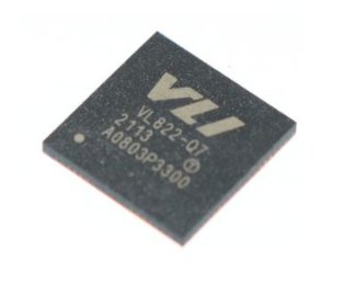
VL822-Q5
USB 3.1 Gen 2
2-Port Hub Controller
QFN56
V
VLI
VL822-Q7
V
VLI
VL822-Q8
USB 3.1 Gen 2
4-Port Hub Controller
USB 3.1 Gen 2
4-Port Hub Controller
w/ USB-C™ Support
QFN-76
QFN-88
�VL822 USB 3.1 Gen2 Hub Controller
Revision History
Rev
Date
0.90
12/26/2018
Note
First Preliminary Release
Initial
EC
-2-
�VL822 USB 3.1 Gen2 Hub Controller
Contents
Revision History ........................................................................................... 2
Contents ..................................................................................................... 3
List of Figures .............................................................................................. 3
Product Features .......................................................................................... 4
VL822 System Overview ............................................................................... 5
USB Battery Charging Behavior ..................................................................... 8
Pinout (VL822-Q7) ....................................................................................... 9
Pin List (VL822-Q7) ..................................................................................... 10
Pin Descriptions (VL822-Q7) ......................................................................... 11
Pinout (VL822-Q8) ...................................................................................... 14
Pin List (VL822-Q8) ..................................................................................... 15
Pin Descriptions (VL822-Q8) ......................................................................... 16
Pinout (VL822-Q5) ...................................................................................... 20
Pin List (VL822-Q5) ..................................................................................... 21
Pin Descriptions (VL822-Q5) ......................................................................... 22
Electrical Specification.................................................................................. 25
Timing Requirements for SPI Flash ................................................................ 26
General Reflow Profile Guidelines ................................................................... 27
Package Mechanical Specifications (VL822-Q7) ............................................... 28
Package Mechanical Specifications (VL822-Q8) ............................................... 29
Package Mechanical Specifications (VL822-Q5) ............................................... 30
Package Top Side Marking & Ordering Information ........................................... 31
List of Figures
Figure 1 – VL822-Q7 Block Diagram ............................................................... 6
Figure 2 – VL822-Q8 Block Diagram ............................................................... 6
Figure 3 – VL822-Q5 Block Diagram ............................................................... 7
Figure 4 – VL822-Q7 Pin Diagram .................................................................. 9
Figure 5 – VL822-Q8 Pin Diagram.................................................................. 14
Figure 6 – VL822-Q5 Pin Diagram.................................................................. 20
Figure 7 – SPI Timing .................................................................................. 26
Figure 8 – Reflow ........................................................................................ 27
Figure 9 – Mechanical Specification – Q7 (QFN 76L 9x9x0.85 mm) Package ........ 28
Figure 10 – Mechanical Specification – Q8 (QFN 88L 10x10x0.85 mm) Package .. 29
Figure 11 – Mechanical Specification – Q5 (QFN 56L 7x7x0.85 mm) Package ...... 30
Figure 12 –Package Top Side Marking ............................................................ 31
-3-
�VL822 USB 3.1 Gen2 Hub Controller
Product Features
VL822-Q8 / VL822-Q7 / VL822-Q5
USB 3.1 Gen2 SuperSpeed Plus 4/2-Port USB Hub Controller
USB 3.1 Compliant
– Compliant to Universal Serial Bus 3.1 Specification
– SuperSpeed Plus USB (USB 3.1 Gen2)
– Compliant to Universal Serial Bus 2.0 Specification
– USB 2.0 Hub Supports MTT
– Supports Simultaneous Operation of Any Combination of SuperSpeed Plus, SuperSpeed, High-Speed, Full-Speed, and
Low-Speed Devices
– Supports USB Power Saving Features such as Link Power Management, Ux States, Selective Suspend, and Function
Suspend
– In-house USB PHY employs advanced CMOS process for low power consumption
USB Type-C 1.0 Rev 1.2 Compliant
– Compliant to USB Type-C Specification Rev 1.3
– VL822-Q8: Integrated 10Gbps Mux for UFP and 2x DFP
– Requires External CC Logic Controller for Orientation Detection/Vconn (Such as VP246 or VP225)
– Additional USB-C DFP support requires separate CC Logic and Mux
Integrated USB Devices
– USB Billboard Class 1.21 Device
Implemented as a USB 2.0 Virtual Device
Configurable Behavior – Expose When Necessary / Always Present / Disabled
– USB HID Class Device
Implemented as a USB 2.0 Virtual Device, Facilitates FW Update or Media Control Buttons
Configurable Behavior – Always Present / Disabled
Full Sideband Signal Support
– Supports Any Combination of Individual or Ganged Mode Over-Current for All Ports
– Supports PWM LED Status Lights
– SPI Interface for Firmware.
– Firmware Upgradable over USB
Comprehensive USB Battery Charging Support
– Supports USB Battery Charging Specification v1.2 (SDP, CDP, DCP)
– Support for Vendor Specific Charging Modes eg. Apple 2.4A, Samsung, etc.
– Supports YD/T 1591-2009
– Supports Stand-Alone Charging when System is Suspend, Shut Down, or Disconnected
– Any Combination of DFPs can be Configured to Support USB Battery Charging
Power and Package
– Requires 3.3V and 1.05V Inputs
– VL822-Q8: QFN 88L green package (10x10x0.85 mm)
– VL822-Q7: QFN 76L green package (9x9x0.85 mm)
– VL822-Q5: QFN 56L green package (7x7x0.85 mm)
– Pin Compatibility with VL820
– 25MHz Xtal
-4-
�VL822 USB 3.1 Gen2 Hub Controller
VL822 System Overview
VIA Lab’s VL822 is USB 3.1 Gen2 Hub Controller and it features highly integrated, application specific design. VL822 features
1x upstream port and 4x/2x downstream ports, all of which support 10Gbps USB 3.1 Gen2 operation. The downstream ports
can support any combination of SuperSpeed Plus (10Gbps), SuperSpeed (5Gbps), High Speed (480Mbps), Full Speed
(12Mbps), and Low Speed (1.5Mbps) devices. VL822’s integrated USB 2.0 hub features Multiple Transaction Translators,
providing increased bandwidth and performance when multiple Full Speed devices are simultaneously used.
VL822 comes in three variants: VL822-Q8 utilizes the QFN88 10x10x0.85 mm package while the VL822-Q7 utilizes the
smaller QFN76 9x9x0.85mm package and VL822-Q5 utilizes the smaller QFN56 7x7x0.85mm package for two port configure.
The larger QFN88 variant features integrated 10Gbps Muxes for the Upstream Facing Port and two Downstream Facings Ports
whereas the smaller QFN76/QFN56 variant does not. The integrated 10Gbps Muxes are ideal for Data-Only USB-C
applications that would otherwise require an external Mux, with the advantage of potential board area savings and improved
signal integrity. If additional USB-C Ports are need, separate CC Logic and Mux solutions.
VL822 features an optionally configurable USB Billboard Device when used in USB-PD Alternate Mode applications, and an
optionally configurable USB HID endpoint to support Media Control Buttons such as Play/Pause, Volume Up/Down, etc.
VL822 features flexible firmware architecture, providing a framework for custom functions in addition to in-field updates. Various
parameters including USB configuration, Tx equalization setting, and GPIO behavior are changeable via firmware. VL822 also
features an optionally configurable USB Charging Controller for charging various devices such as smartphones and tablets that
can be configure on a per-port basis.
VL822-based hub devices work under Windows, Mac OS X, and various Linux kernels without additional drivers. VL822-based
hub devices are also compatible with non-x86 devices and platforms that support USB hub functions such as smart phones,
tablets, and set-top boxes. It is well suited for all USB hub applications such as standalone USB hubs, Notebook/Ultrabook
docking stations/port-replicators, desktop PC front panel, motherboard on-board hub, and USB hub compound devices.
-5-
�VL822 USB 3.1 Gen2 Hub Controller
Figure 1 – VL822-Q7 Block Diagram
Figure 2 – VL822-Q8 Block Diagram
-6-
�VL822 USB 3.1 Gen2 Hub Controller
Figure 3 – VL822-Q5 Block Diagram
-7-
�VL822 USB 3.1 Gen2 Hub Controller
USB Battery Charging Behavior
3 Concepts of Rapid Charging over USB:
Rapid Charging over USB enables charging of devices at rates in excess of baseline USB standards.
The current limit of USB 2.0 is 500mA for configured devices, and the current limit of USB 3.0 is 900mA for configured
devices. Depending on the device, Rapid Charging implementations typically feature current limits between 1000mA to
2400mA.
It is the Host/Hub’s responsibility to advertise Rapid Charging capabilities, and it is the Device’s responsibility
to recognize and determine those capabilities.
Rapid Charging over USB enables charging at rates in excess of baseline USB specifications, so in order to prevent a
situation where a device sinks more current than what a port is rated for, different manufacturers employ various charging
schemes in an attempt to ensure safe and reliable operation with their respective device and charger. It goes without saying
that Rapid Charging will only occur when both Host/Hub and Device supports it.
The rate at which a device charges is dependent upon the device.
This means that the device must determine the host/hub port’s capabilities to determine which charging mode to use. Also,
the rate at which a device charges can vary depending on the status of the device. For example, some devices only charge
at their maximum rate when the battery is nearly depleted. When the battery is nearly full, they may switch to a tricklecharge mode. The Host/Hub rapid-charging port has no control over this behavior.
Supported USB Charging Modes
SDP – Standard Downstream Port
This is a typical USB 2.0 or USB 3.0 port and does not explicitly support Rapid USB Charging. SDP is constrained to the
current limits as defined in the USB 2.0 or USB 3.0 spec which are 500mA and 900mA respectively. While the actual current
limit is enforced by the polyfuse or power-switch providing current-limiting functionality for the downstream port, most USB
devices will not draw more than 500mA or 900mA under USB 2.0 or USB 3.0 modes.
CDP – Charging Downstream Port
CDP is defined in the USB Battery Charging Specification 1.2 and enables devices that are able to correctly recognize CDP to
simultaneously function as a USB device while drawing up to 1.5A for Rapid Charging when connected to the downstream
port of a USB Host or Hub that advertises CDP capability.
DCP – Dedicated Charging Port
DCP is defined in the USB Battery Charging Specification 1.2 and has been in use on an unofficial basis prior to the official
USB Battery Charging Specification. DCP is a dedicated charging mode, so when a device is charging under DCP, regular USB
operations such as data transfer to the device are not supported.
Special Modes
Various vendors such as Apple, RIM, Motorola, etc. may employ different detection mechanisms compared to other USB
devices and thus, may enter Rapid Charging under the previously mentioned charging modes. VL822 supports an auto
detection mechanism that provides charging for the majority of devices.
-8-
�VL822 USB 3.1 Gen2 Hub Controller
Pinout (VL822-Q7)
Figure 4 – VL822-Q7 Pin Diagram
-9-
�VL822 USB 3.1 Gen2 Hub Controller
Pin List (VL822-Q7)
Table 1 – VL822-Q7 Pin List
Pin
Pin Name
Pin
Pin Name
1
USBOC1
39
USBPE4
2
USBPE1
40
USBOC4
3
SSTX1+
41
USBOC0
4
SSTX1–
42
USBPE0
5
VCC10I
43
VBUSDET0
6
SSRX1+
44
USB3XO
7
SSRX1–
45
USB3XI
8
VCC10I
46
VCC33I
9
HSD1+
47
REXT
10
HSD1–
48
VDD
11
VDD
49
SSTX0–
12
SSTX2+
50
SSTX0+
13
SSTX2–
51
VCC10I
14
VCC10I
52
SSRX0–
15
SSRX2+
53
SSRX0+
16
SSRX2–
54
VCC10I
17
VCC33I
55
HSD0+
18
HSD2+
56
HSD0–
19
HSD2–
57
GPIO0/HID0
20
USBOC3
58
GPIO1/HID1
21
USBPE3
59
GPIO2/HID2
22
HSD3+
60
GPIO3/HID3
23
HSD3–
61
GPIO4/HID4
24
VCC33I
62
VCC33I
25
SSTX3+
63
GPIO5/EXTPWRON/WAKE
26
SSTX3–
64
GPIO6 / USBSUS
27
VCC10I
65
GPIO7 / SMDAT
28
SSRX3+
66
GPIO8 / SMCLK
29
SSRX3–
67
VDD
30
VDD
68
RESET#
31
SSTX4+
69
USBLED1 / SPISI
32
SSTX4–
70
USBLED2 / SPICK
33
VCC10I
71
USBLED3 / SPISO
34
SSRX4+
72
USBLED4 / SPICS
35
SSRX4–
73
VCC33I
36
VCC10I
74
TESTEN
37
HSD4+
75
USBOC2
38
HSD4–
76
USBPE2
- 10 -
�VL822 USB 3.1 Gen2 Hub Controller
Pin Descriptions (VL822-Q7)
Signal Type Definition
Name
Type
Signal Description
Input
I
A logic input-only signal
Output
O
A logic output only signal
Input/ Output
I/O
A logic bi-directional signal
Power
PWR
A power pin
Ground
GND
A ground pin
USB 3.1 Interface
Pin Name
Pin #
I/O
Signal Description
SSTX0-
49
O
USB 3.1 UFP Differential TX–
SSTX0+
50
O
USB 3.1 UFP Differential TX+
SSRX0-
52
I
USB 3.1 UFP Differential RX–
SSRX0+
53
I
USB 3.1 UFP Differential RX+
SSTX1+
3
O
USB 3.1 DFP1 Differential TX+
SSTX1-
4
O
USB 3.1 DFP1 Differential TX–
SSRX1+
6
I
USB 3.1 DFP1 Differential RX+
SSRX1-
7
I
USB 3.1 DFP1 Differential RX–
SSTX2+
12
O
USB 3.1 DFP2 Differential TX+
SSTX2-
13
O
USB 3.1 DFP2 Differential TX–
SSRX2+
15
I
USB 3.1 DFP2 Differential RX+
SSRX2-
16
I
USB 3.1 DFP2 Differential RX–
SSTX3+
25
O
USB 3.1 DFP3 Differential TX+
SSTX3-
26
O
USB 3.1 DFP3 Differential TX–
SSRX3+
28
I
USB 3.1 DFP3 Differential RX+
SSRX3-
29
I
USB 3.1 DFP3 Differential RX–
SSTX4+
31
O
USB 3.1 DFP4 Differential TX+
SSTX4-
32
O
USB 3.1 DFP4 Differential TX–
SSRX4+
34
I
USB 3.1 DFP4 Differential RX+
SSRX4-
35
I
USB 3.1 DFP4 Differential RX–
Analog Command Block
Pin Name
Pin #
I/O
Signal Description
USB3XO
44
O
25M Crystal Output
USB3XI
45
I
25M Crystal Input
REXT
47
I
Connect to External Reference Resistor (12.4K+/- 1%)
- 11 -
�VL822 USB 3.1 Gen2 Hub Controller
Test Pin
Pin Name
Pin #
I/O
TESTEN
74
I
GPIO7 / SMDAT
65
I/O
GPIO8 / SMCLK
66
I/O
Signal Description
Test Mode Enable
Low: Normal mode.
High: Test mode.
Available for GPIO Use, Config via Firmware Setting.
SMBus data with Proprietary Data Format. (Open Drain)
Available for GPIO Use, Config via Firmware Setting.
SMBus clock with Proprietary Data Format. (Open Drain)
USB 2.0 Interface
Pin Name
Pin #
I/O
Signal Description
HSD0+
55
I/O
USB 2.0 UFP Differential D+
HSD0–
56
I/O
USB 2.0 UFP Differential D–
HSD1+
9
I/O
USB 2.0 DFP1 Differential D+
HSD1–
10
I/O
USB 2.0 DFP1 Differential D–
HSD2+
18
I/O
USB 2.0 DFP2 Differential D+
HSD2–
19
I/O
USB 2.0 DFP2 Differential D–
HSD3+
22
I/O
USB 2.0 DFP3 Differential D+
HSD3–
23
I/O
USB 2.0 DFP3 Differential D–
HSD4+
37
I/O
USB 2.0 DFP4 Differential D+
HSD4–
38
I/O
USB 2.0 DFP4 Differential D–
Power and Ground
Pin Name
Pin #
I/O
Signal Description
GND
EPAD
GND
Ground
VDD
11, 30, 48, 67
PWR
1.05V Core Power
PWR
1.05V Analog Power
PWR
3.3V Analog Power
VCC10I
VCC33I
5, 8, 14, 27, 33, 36, 51,
54
17, 24, 46, 62, 73
Side Band Signal and Miscellaneous
Pin Name
Pin #
I/O
USBOC0
41
I or I/O
USBPE0
42
O
USBOC1
1
I or I/O
USBPE1
2
O
Signal Description
UFP Over Current Detection
Open Drain (3.3V Max); Pin must be pulled high if NC.
High: Normal
Low: Port Over Current Event
UFP USB PE
USB Power Enable Mode
High: Enable
Low: Off
DFP1 Over Current Detection
Open Drain (3.3V Max); Pin must be pulled high if NC.
High: Normal
Low: Port Over Current Event
DFP1 USB PE
USB Power Enable Mode
High: Enable
Low: Off
- 12 -
�VL822 USB 3.1 Gen2 Hub Controller
Side Band Signal and Miscellaneous
Pin Name
Pin #
I/O
USBOC2
75
I or I/O
USBPE2
76
O
USBOC3
20
I or I/O
USBPE3
21
O
USBPE4
39
I or I/O
USBOC4
40
O
GPIO0 / HID0
57
I/O
GPIO1 / HID1
58
I/O
GPIO2 / HID2
59
I/O
GPIO3 / HID3
60
I/O
GPIO4 / HID4
61
I/O
GPIO5 / EXTPWRON /
WAKE
63
I/O
GPIO6 / USBSUS
64
I/O
RESET#
68
I
USBLED1 / SPISI
69
I/O
USBLED2 / SPICLK
70
I/O
USBLED3 / SPISO
71
I/O
USBLED4 / SPICS
72
I/O
VBUSDET0
43
I
Signal Description
DFP2 Over Current Detection
Open Drain (3.3V Max); Pin must be pulled high if NC.
High: Normal
Low: Port Over Current Event
DFP2 USB PE
USB Power Enable Mode
High: Enable
Low: Off
DFP3 Over Current Detection
Open Drain (3.3V Max); Pin must be pulled high if NC.
High: Normal
Low: Port Over Current Event
DFP3 USB PE
USB Power Enable Mode
High: Enable
Low: Off
DFP4 USB PE
USB Power Enable Mode
High: Enable
Low: Off
DFP4 Over Current Detection
Open Drain (3.3V Max); Pin must be pulled high if NC.
High: Normal
Low: Port Over Current Event
GPIO / HID Shared Pin.
Available for GPIO Use, Config via Firmware Setting.
Available for HID button Use, Config via Firmware Setting.
GPIO / HID Shared Pin.
Available for GPIO Use, Config via Firmware Setting.
Available for HID button Use, Config via Firmware Setting.
GPIO / HID Shared Pin.
Available for GPIO Use, Config via Firmware Setting.
Available for HID button Use, Config via Firmware Setting.
GPIO / HID Shared Pin.
Available for GPIO Use, Config via Firmware Setting.
Available for HID button Use, Config via Firmware Setting.
GPIO / HID Shared Pin.
Available for GPIO Use, Config via Firmware Setting.
Available for HID button Use, Config via Firmware Setting.
GPIO / External Power Status / Wake Shared pin.
Available for GPIO Use, Config via Firmware Setting.
DC Jack Power Source Insert Detection (3.3V Max)
Available for Connected Standby use,
Config via Firmware Setting.
GPIO
Available for GPIO Use, Config via Firmware Setting.
Reset Input of Hub Controller
Low: Reset
High: Normal Operation
Power On sequence, Refer to Appendix-1.
DFP1 LED Indicator / SPISI shared pin.
Active High Output for LED Use.
DFP2 LED Indicator / SPISCLK shared pin.
Active High Output for LED Use.
DFP3 LED Indicator / SPISO shared pin.
Active High Output for LED Use.
DFP4 LED Indicator / SPICS shared pin.
Active High Output for LED Use
UFP Vbus Detection (3.3V Max)
- 13 -
�VL822 USB 3.1 Gen2 Hub Controller
Pinout (VL822-Q8)
Figure 5 – VL822-Q8 Pin Diagram
- 14 -
�VL822 USB 3.1 Gen2 Hub Controller
Pin List (VL822-Q8)
Table 2 – VL822-Q8 Pin List
Pin
Pin Name
Pin
Pin Name
1
SSTX1A+
45
USBPE4
2
SSTX1A–
46
USBOC4
3
SSTX1B–
47
USBOC0
4
SSTX1B+
48
USBPE0
5
VCC10I
49
VBUSDET0
6
SSRX1A+
50
USB3XO
7
SSRX1A–
51
USB3XI
8
SSRX1B–
52
VCC33I
9
SSRX1B+
53
REXT
10
VCC10I
54
VDD
11
HSD1+
55
SSTX0A+
12
HSD1–
56
SSTX0A–
13
VDD
57
SSTX0B–
14
SSTX2+
58
SSTX0B+
15
SSTX2–
59
VCC10I
16
VCC10I
60
SSRX0A+
17
SSRX2+
61
SSRX0A–
18
SSRX2–
62
SSRX0B–
19
VCC33I
63
SSRX0B+
20
HSD2+
64
VCC10I
21
HSD2–
65
HSD0+
22
USBOC3
66
HSD0–
23
USBPE3
67
GPIO0/HID0/ATT0
24
HSD3+
68
GPIO1/HID1/ORI0
25
HSD3–
69
GPIO2/HID2/ATT1
26
VCC33I
70
GPIO3/HID3/ORI1
27
SSTX3+
71
GPIO4/HID4/ATT4
28
SSTX3–
72
VCC33I
29
VCC10I
73
GPIO5/EXTPWRON/WAKE/ORI4
30
SSRX3+
74
GPIO6
31
SSRX3–
75
GPIO7 / SMDAT
32
VDD
76
GPIO8 / SMCLK
33
SSTX4A+
77
VDD
34
SSTX4A–
78
RESET#
35
SSTX4B–
79
USBLED1 / SPISI
36
SSTX4B+
80
USBLED2 / SPICK
37
VCC10I
81
USBLED3 / SPISO
38
SSRX4A+
82
USBLED4 / SPICS
39
SSRX4A–
83
VCC33I
40
SSRX4B–
84
TESTEN
41
SSRX4B+
85
USBOC2
42
VCC10I
86
USBPE2
43
HSD4+
87
USBOC1
44
HSD4–
88
USBPE1
- 15 -
�VL822 USB 3.1 Gen2 Hub Controller
Pin Descriptions (VL822-Q8)
Signal Type Definition
Name
Type
Signal Description
Input
I
A logic input-only signal
Output
O
A logic output only signal
Input/ Output
I/O
A logic bi-directional signal
Power
PWR
A power pin
Ground
GND
A ground pin
Pin Name
Pin #
I/O
Signal Description
SSTX0A+
55
O
USB 3.1 UFP Differential TX+; Side A
SSTX0A-
56
O
USB 3.1 UFP Differential TX–; Side A
SSTX0B-
57
O
USB 3.1 UFP Differential TX–; Side B
SSTX0B+
58
O
USB 3.1 UFP Differential TX+; Side B
SSRX0A+
60
I
USB 3.1 UFP Differential RX+; Side A
SSRX0A-
61
I
USB 3.1 UFP Differential RX–; Side A
SSRX0B-
62
I
USB 3.1 UFP Differential RX–; Side B
SSRX0B+
63
I
USB 3.1 UFP Differential RX+; Side B
SSTX1A+
1
O
USB 3.1 DFP1 Differential TX+; Side A
SSTX1A-
2
O
USB 3.1 DFP1 Differential TX–; Side A
SSTX1B-
3
O
USB 3.1 DFP1 Differential TX–; Side B
SSTX1B+
4
O
USB 3.1 DFP1 Differential TX+; Side B
SSRX1A+
6
I
USB 3.1 DFP1 Differential RX+; Side A
SSRX1A-
7
I
USB 3.1 DFP1 Differential RX–; Side A
SSRX1B-
8
I
USB 3.1 DFP1 Differential RX–; Side B
SSRX1B+
9
I
USB 3.1 DFP1 Differential RX+; Side B
SSTX2+
14
O
USB 3.1 DFP2 Differential TX+
SSTX2-
15
O
USB 3.1 DFP2 Differential TX–
SSRX2+
17
I
USB 3.1 DFP2 Differential RX+
SSRX2-
18
I
USB 3.1 DFP2 Differential RX–
SSTX3+
27
O
USB 3.1 DFP3 Differential TX+
SSTX3-
28
O
USB 3.1 DFP3 Differential TX–
SSRX3+
30
I
USB 3.1 DFP3 Differential RX+
SSRX3-
31
I
USB 3.1 DFP3 Differential RX–
SSTX4A+
33
O
USB 3.1 DFP4 Differential TX+; Side A
SSTX4A-
34
O
USB 3.1 DFP4 Differential TX–; Side A
SSTX4B-
35
O
USB 3.1 DFP4 Differential TX–; Side B
SSTX4B+
36
O
USB 3.1 DFP4 Differential TX+; Side B
SSRX4A+
38
I
USB 3.1 DFP4 Differential RX+; Side A
SSRX4A-
39
I
USB 3.1 DFP4 Differential RX–; Side A
SSRX4B-
40
I
USB 3.1 DFP4 Differential RX–; Side B
SSRX4B+
41
I
USB 3.1 DFP4 Differential RX+; Side B
USB 3.1 Interface
- 16 -
�VL822 USB 3.1 Gen2 Hub Controller
USB 2.0 Interface
Pin Name
Pin #
I/O
Signal Description
HSD0+
65
I/O
USB 2.0 UFP Differential D+
HSD0–
66
I/O
USB 2.0 UFP Differential D–
HSD1+
11
I/O
USB 2.0 DFP1 Differential D+
HSD1–
12
I/O
USB 2.0 DFP1 Differential D–
HSD2+
20
I/O
USB 2.0 DFP2 Differential D+
HSD2–
21
I/O
USB 2.0 DFP2 Differential D–
HSD3+
24
I/O
USB 2.0 DFP3 Differential D+
HSD3–
25
I/O
USB 2.0 DFP3 Differential D–
HSD4+
43
I/O
USB 2.0 DFP4 Differential D+
HSD4–
44
I/O
USB 2.0 DFP4 Differential D–
Analog Command Block
Pin Name
Pin #
I/O
Signal Description
USB3XO
50
O
25M Crystal Output
USB3XI
51
I
25M Crystal Input
REXT
53
I
Connect to External Reference Resistor (12.4K+/- 1%)
Pin Name
Pin #
I/O
Signal Description
GND
EPAD
GND
Ground
VDD
13,32,54, 77
5, 10, 16, 29,
37, 42, 59. 64,
19, 26, 52, 72,
83
PWR
1.05V Core Power
PWR
1.05V Analog Power
PWR
3.3V Analog Power
Pin Name
Pin #
I/O
TESTEN
84
I
GPIO7 / SMDAT
75
I/O
GPIO8 / SMCLK
76
I/O
Signal Description
Test Mode Enable
Low: Normal mode.
High: Test mode.
Available for GPIO Use, Config via Firmware Setting.
SMBus data with Proprietary Data Format. (Open Drain)
Available for GPIO Use, Config via Firmware Setting.
SMBus clock with Proprietary Data Format. (Open Drain)
Power and Ground
VCC10I
VCC33I
Test Pin
- 17 -
�VL822 USB 3.1 Gen2 Hub Controller
Side Band Signal and Miscellaneous
Pin Name
Pin #
I/O
USBOC0
47
I or I/O
USBPE0
48
O
USBOC1
87
I or I/O
USBPE1
88
O
USBOC2
85
I or I/O
USBPE2
86
O
USBOC3
22
I or I/O
USBPE3
23
O
USBPE4
45
I or I/O
USBOC4
46
O
Signal Description
UFP Over Current Detection
Open Drain (3.3V Max); Pin must
High: Normal
Low: Port Over Current Event
UFP USB PE
USB Power Enable Mode
High: Enable
Low: Off
DFP1 Over Current Detection
Open Drain (3.3V Max); Pin must
High: Normal
Low: Port Over Current Event
DFP1 USB PE
USB Power Enable Mode
High: Enable
Low: Off
DFP2 Over Current Detection
Open Drain (3.3V Max); Pin must
High: Normal
Low: Port Over Current Event
DFP2 USB PE
USB Power Enable Mode
High: Enable
Low: Off
DFP3 Over Current Detection
Open Drain (3.3V Max); Pin must
High: Normal
Low: Port Over Current Event
DFP3 USB PE
USB Power Enable Mode
High: Enable
Low: Off
DFP4 USB PE
USB Power Enable Mode
High: Enable
Low: Off
DFP4 Over Current Detection
Open Drain (3.3V Max); Pin must
High: Normal
Low: Port Over Current Event
- 18 -
be pulled high if NC.
be pulled high if NC.
be pulled high if NC.
be pulled high if NC.
be pulled high if NC.
�VL822 USB 3.1 Gen2 Hub Controller
Side Band Signal and Miscellaneous
Pin Name
Pin #
I/O
GPIO0 / HID0 / ATT0
67
I/O
GPIO1 / HID1 / ORI0
68
I/O
GPIO2 / HID2 / ATT1
69
I/O
GPIO3 / HID3 / ORI1
70
I/O
GPIO4 / HID4 / ATT4
71
I/O
GPIO5 / EXTPWRON /
WAKE / ORI4
73
I/O
GPIO6
74
I/O
RESET#
78
I
USBLED1/SPISI
79
I/O
USBLED2/SPICLK
80
I/O
USBLED3/SPISO
81
I/O
USBLED4/SPICS
82
I/O
VBUSDET0
49
I
Signal Description
GPIO / HID Shared Pin.
Available for GPIO Use, Config via Firmware Setting.
Available for HID button Use, Config via Firmware Setting.
UFP Host Attach Status Input Pin, Refer to Appendix-2.
GPIO / HID Shared Pin.
Available for GPIO Use, Config via Firmware Setting.
Available for HID button Use, Config via Firmware Setting.
UFP Mux Orientation Setting Input Pin, Refer to Appendix-2.
GPIO / HID Shared Pin.
Available for GPIO Use, Config via Firmware Setting.
Available for HID button Use, Config via Firmware Setting.
DFP1 Device Attach Status Input Pin, Refer to Appendix-2.
GPIO / HID Shared Pin.
Available for GPIO Use, Config via Firmware Setting.
Available for HID button Use, Config via Firmware Setting.
DFP1 Mux Orientation Setting Input Pin, Refer to Appendix-2.
GPIO / HID Shared Pin.
Available for GPIO Use, Config via Firmware Setting.
Available for HID button Use, Config via Firmware Setting.
DFP4 Device Attach Status Input Pin, Refer to Appendix-2.
GPIO / External Power Status / Wake Shared pin.
Available for GPIO Use, Config via Firmware Setting.
DC Jack Power Source Insert Detection (3.3V Max).
Available for Connected Standby use, Config via Firmware Setting.
DFP4 Mux Orientation Setting Input Pin, Refer to Appendix-2.
GPIO
Available for GPIO Use, Config via Firmware Setting.
Reset Input of Hub Controller
Low: Reset
High: Normal Operation
Power On sequence, Refer to Appendix-1.
DFP1 LED Indicator / SPISI shared pin.
Active High Output for LED Use.
DFP2 LED Indicator / SPISCLK shared pin.
Active High Output for LED Use.
DFP3 LED Indicator / SPISO shared pin.
Active High Output for LED Use.
DFP4 LED Indicator / SPICS shared pin.
Active High Output for LED Use
UFP Vbus Detection (3.3V Max)
- 19 -
�VL822 USB 3.1 Gen2 Hub Controller
Pinout (VL822-Q5)
Figure 6 – VL822-Q5 Pin Diagram
- 20 -
�VL822 USB 3.1 Gen2 Hub Controller
Pin List (VL822-Q5)
Table 3 – VL822-Q5 Pin List
Pin
Pin Name
Pin
Pin Name
1
SSTX1+
29
VCC33I
2
SSTX1–
30
REXT
3
VCC10I
31
VDD
4
SSRX1+
32
SSTX0–
5
SSRX1–
33
SSTX0+
6
VCC10I
34
VCC10I
7
HSD1+
35
SSRX0–
8
HSD1–
36
SSRX0+
9
VDD
37
VCC10I
10
SSTX2+
38
HSD0+
11
SSTX2–
39
HSD0–
12
VCC10I
40
GPIO0/HID0
13
SSRX2+
41
VCC33I
14
SSRX2–
42
GPIO6 / USBSUS
15
VCC33I
43
GPIO7 / SMDAT
16
HSD2+
44
GPIO8 / SMCLK
17
HSD2–
45
VDD
18
GPIO/SDA3
46
RESET#
19
GPIO/SCL3
47
USBLED1 / SPISI
20
VCC33I
48
USBLED2 / SPICK
21
VCC10I
49
SPISO
22
VDD
50
SPICS
23
VCC10I
51
VCC33I
24
USB3XI
52
TESTEN
25
USB3XO
53
USBOC2
26
VBUSDET0
54
USBPE2
27
GPIO/SCL4
55
USBOC1
28
GPIO/SDA4
56
USBPE1
- 21 -
�VL822 USB 3.1 Gen2 Hub Controller
Pin Descriptions (VL822-Q5)
Signal Type Definition
Name
Type
Signal Description
Input
I
A logic input-only signal
Output
O
A logic output only signal
Input/ Output
I/O
A logic bi-directional signal
Power
PWR
A power pin
Ground
GND
A ground pin
USB 3.1 Interface
Pin Name
Pin #
I/O
Signal Description
SSTX0-
32
O
USB 3.1 UFP Differential TX–
SSTX0+
33
O
USB 3.1 UFP Differential TX+
SSRX0-
35
I
USB 3.1 UFP Differential RX–
SSRX0+
36
I
USB 3.1 UFP Differential RX+
SSTX1+
1
O
USB 3.1 DFP1 Differential TX+
SSTX1-
2
O
USB 3.1 DFP1 Differential TX–
SSRX1+
4
I
USB 3.1 DFP1 Differential RX+
SSRX1-
5
I
USB 3.1 DFP1 Differential RX–
SSTX2+
10
O
USB 3.1 DFP2 Differential TX+
SSTX2-
11
O
USB 3.1 DFP2 Differential TX–
SSRX2+
13
I
USB 3.1 DFP2 Differential RX+
SSRX2-
14
I
USB 3.1 DFP2 Differential RX–
Analog Command Block
Pin Name
Pin #
I/O
Signal Description
USB3XO
25
O
25M Crystal Output
USB3XI
24
I
25M Crystal Input
REXT
30
I
Connect to External Reference Resistor (12.4K+/- 1%)
- 22 -
�VL822 USB 3.1 Gen2 Hub Controller
Test Pin
Pin Name
Pin #
I/O
TESTEN
52
I
GPIO7 / SMDAT
43
I/O
GPIO8 / SMCLK
44
I/O
Signal Description
Test Mode Enable
Low: Normal mode.
High: Test mode.
Available for GPIO Use, Config via Firmware Setting.
SMBus data with Proprietary Data Format. (Open Drain)
Pin must be pulled high if NC.
Available for GPIO Use, Config via Firmware Setting.
SMBus clock with Proprietary Data Format. (Open Drain)
Pin must be pulled high if NC.
USB 2.0 Interface
Pin Name
Pin #
I/O
Signal Description
HSD0+
38
I/O
USB 2.0 UFP Differential D+
HSD0–
39
I/O
USB 2.0 UFP Differential D–
HSD1+
7
I/O
USB 2.0 DFP1 Differential D+
HSD1–
8
I/O
USB 2.0 DFP1 Differential D–
HSD2+
16
I/O
USB 2.0 DFP2 Differential D+
HSD2–
17
I/O
USB 2.0 DFP2 Differential D–
Power and Ground
Pin Name
Pin #
I/O
Signal Description
GND
EPAD
GND
Ground
VDD
9, 22, 31, 45
PWR
1.05V Core Power
VCC10I
3, 6, 12, 21, 23, 34, 37
PWR
1.05V Analog Power
VCC33I
15, 20, 29, 41, 51
PWR
3.3V Analog Power
Side Band Signal and Miscellaneous
Pin Name
Pin #
I/O
USBOC1
55
I or I/O
USBPE1
56
O
USBOC2
53
I or I/O
USBPE2
54
O
Signal Description
DFP1 Over Current Detection
Open Drain (3.3V Max); Pin must be pulled high if NC.
High: Normal
Low: Port Over Current Event
DFP1 USB PE
USB Power Enable Mode
High: Enable
Low: Off
DFP2 Over Current Detection
Open Drain (3.3V Max); Pin must be pulled high if NC.
High: Normal
Low: Port Over Current Event
DFP2 USB PE
USB Power Enable Mode
High: Enable
Low: Off
- 23 -
�VL822 USB 3.1 Gen2 Hub Controller
Side Band Signal and Miscellaneous
Pin Name
Pin #
I/O
Signal Description
GPIO0 / HID0
40
I/O
GPIO6 / USBSUS
42
I/O
RESET#
46
I
USBLED1 / SPISI
47
I/O
USBLED2 / SPICLK
48
I/O
SPISO
49
I/O
SPISO pin.
SPICS
50
I/O
SPICS pin.
VBUSDET0
26
I
UFP Vbus Detection (3.3V Max)
GPIO / HID Shared Pin.
Available for GPIO Use, Config via Firmware Setting.
Available for HID button Use, Config via Firmware Setting.
GPIO
Available for GPIO Use, Config via Firmware Setting.
Reset Input of Hub Controller
Low: Reset
High: Normal Operation
Power On sequence, Refer to Appendix-1.
DFP1 LED Indicator / SPISI shared pin.
Active High Output for LED Use.
DFP2 LED Indicator / SPISCLK shared pin.
Active High Output for LED Use.
GPIO/SDA3
18
I or I/O
GPIO / I2C Data Shared Pin.
Available for GPIO Use, Config via Firmware Setting.
Available for I2C Use, Config via Firmware Setting.
Open Drain (3.3V Max); Pin must be pulled high if NC.
GPIO/SCL3
19
O
GPIO / I2C Clock Shared Pin.
Available for GPIO Use, Config via Firmware Setting.
Available for I2C Use, Config via Firmware Setting.
GPIO/SDA4
28
I or I/O
GPIO / I2C Data Shared Pin.
Available for GPIO Use, Config via Firmware Setting.
Available for I2C Use, Config via Firmware Setting.
Open Drain (3.3V Max); Pin must be pulled high if NC.
GPIO/SCL4
27
O
GPIO / I2C Clock Shared Pin.
Available for GPIO Use, Config via Firmware Setting.
Available for I2C Use, Config via Firmware Setting.
- 24 -
�VL822 USB 3.1 Gen2 Hub Controller
Electrical Specification
Absolute Maximum Rating
Symbol
Parameter
Min
Max
Unit
Note
TSTG
Storage Temperature
-55
125
°C
—
V33
3.3V Power Supply Voltage
-0.5
3.63
V
—
V10
1.05V Input Voltage
-0.5
V
—
VIN
Input voltage at I/O pins
-0.5
1.1
(≦ 3.63) and
(≦ V33+0.3)
V
—
VESD
Electrostatic Discharge
-2000
2000
V
θjc
θja
Thermal resistance between
junction and case
Thermal resistance between
junction and ambient
TBD
°C/W
TBD
°C/W
PD
Power dissipation
—
TBD
Note: Stress above conditions may cause permanent damage to the device.
Functional operation of this device should be restricted to the conditions described.
Human Body
Model
4L PCB
definitions
follow
JESD51-7
W
Note: About thermal factors, Ta is the concerned ambient temperature, and
θca = θja - θjc
TJ = θja * PD + Ta
Tc = θca * PD + Ta
Operating Conditions
Symbol
Parameter
Min
Max
Unit
Note
TA
Ambient Temperature
0
70
°C
—
Tj
Junction Temperature
0
125
°C
—
V33
3.3V Power Supply Voltage
3.0
3.6
V
—
V10
1.05V Input Voltage
1.0
1.1
V
—
VIL
Input Low Voltage
—
0.8
V
—
VIH
Input High Voltage
2.3
—
V
—
VOL
Output Low Voltage
—
0.4
V
IOL=4mA
VOH
Output High Voltage
2.4
—
V
IOH=4mA
IIL
Input Leakage Current
—
+/-10
µA
0