nRF52840 Preview
Development Kit
v0.11.x
User Guide
v1.2
4440_025 v1.2 / 2018-01-19
�Contents
Revision history. . . . . . . . . . . . . . . . . . . . . . . . . . . . . . . . . .
iv
1
Introduction.
5
2
Minimum requirements.
3
Kit content.
. . . . . . . . . . . . . . . . . . . . . . . . . . . . . . . . . .
. . . . . . . . . . . . . . . . . . . . . . . . . . .
6
. . . . . . . . . . . . . . . . . . . . . . . . . . . . . . . . . . .
7
3.1 Hardware content . . . . . . . . . . . . . . . . . . . . . . . . . . . . . . . .
3.2 Downloadable content . . . . . . . . . . . . . . . . . . . . . . . . . . . . . .
3.3 Related documentation . . . . . . . . . . . . . . . . . . . . . . . . . . . . . .
7
7
8
4
Getting started.
9
5
Nordic tools and downloads.
6
Start developing.
7
Interface MCU.
8
. . . . . . . . . . . . . . . . . . . . . . . . . . . . . . . .
. . . . . . . . . . . . . . . . . . . . . . . .
10
. . . . . . . . . . . . . . . . . . . . . . . . . . . . . . .
12
. . . . . . . . . . . . . . . . . . . . . . . . . . . . . . . .
13
7.1 IF Boot/Reset button . . . . . . . . . . . . . . . . . . . . . . . . . . . . . .
7.2 Virtual COM port . . . . . . . . . . . . . . . . . . . . . . . . . . . . . . . .
7.2.1 Dynamic HWFC handling . . . . . . . . . . . . . . . . . . . . . . . . . . .
7.3 Swapping interface MCU firmware . . . . . . . . . . . . . . . . . . . . . . . . .
7.4 MSD . . . . . . . . . . . . . . . . . . . . . . . . . . . . . . . . . . . . .
13
13
14
14
15
Hardware description.
16
. . . . . . . . . . . . . . . . . . . . . . . . . . . .
8.1 Hardware drawings . . . . . . . . . . . . . . . . . . . . . . . . . . . . . . .
8.2 Block diagram . . . . . . . . . . . . . . . . . . . . . . . . . . . . . . . . .
8.3 Power supply . . . . . . . . . . . . . . . . . . . . . . . . . . . . . . . . . .
8.3.1 5 V power sources . . . . . . . . . . . . . . . . . . . . . . . . . . . . . .
8.3.2 VDD power sources . . . . . . . . . . . . . . . . . . . . . . . . . . . . .
8.3.3 Interface MCU power . . . . . . . . . . . . . . . . . . . . . . . . . . . .
8.3.4 nRF52840 power source . . . . . . . . . . . . . . . . . . . . . . . . . . .
8.3.5 nRF52840 direct supply . . . . . . . . . . . . . . . . . . . . . . . . . . . .
8.4 Operating modes . . . . . . . . . . . . . . . . . . . . . . . . . . . . . . . .
8.4.1 USB detect . . . . . . . . . . . . . . . . . . . . . . . . . . . . . . . . .
8.4.2 nRF only mode . . . . . . . . . . . . . . . . . . . . . . . . . . . . . . .
8.4.3 Signal switches . . . . . . . . . . . . . . . . . . . . . . . . . . . . . . .
8.5 External memory . . . . . . . . . . . . . . . . . . . . . . . . . . . . . . . .
8.6 Connector interface . . . . . . . . . . . . . . . . . . . . . . . . . . . . . . .
8.7 Buttons and LEDs . . . . . . . . . . . . . . . . . . . . . . . . . . . . . . . .
8.8 32.768 kHz crystal . . . . . . . . . . . . . . . . . . . . . . . . . . . . . . . .
8.9 Measuring current . . . . . . . . . . . . . . . . . . . . . . . . . . . . . . .
8.9.1 Preparing the development kit board . . . . . . . . . . . . . . . . . . . . . .
8.9.2 Using an oscilloscope for current profile measurement . . . . . . . . . . . . . . .
8.9.3 Using an ampere-meter for current measurement . . . . . . . . . . . . . . . . .
8.10 RF measurements . . . . . . . . . . . . . . . . . . . . . . . . . . . . . . .
8.11 Debug input and trace . . . . . . . . . . . . . . . . . . . . . . . . . . . . .
8.12 Debug output . . . . . . . . . . . . . . . . . . . . . . . . . . . . . . . . .
8.13 NFC antenna interface . . . . . . . . . . . . . . . . . . . . . . . . . . . . .
4440_025 v1.2
ii
16
16
17
18
18
20
21
22
22
22
23
23
25
26
28
29
30
31
31
32
33
34
35
36
�8.14 Extra op-amp . . . . . . . . . . . . . . . . . . . . . . . . . . . . . . . . .
8.15 Solder bridge configuration . . . . . . . . . . . . . . . . . . . . . . . . . . .
37
37
Legal notices. . . . . . . . . . . . . . . . . . . . . . . . . . . . . . . . . . .
40
4440_025 v1.2
iii
�Revision history
Date
Version
Description
January 2018
1.2
Updated to match PDK v0.11.x
February 2017
1.1
Updated:
• Swapping interface MCU firmware on page 14
• MSD on page 15
December 2016
4440_025 v1.2
1.0
First release
iv
�1
Introduction
The nRF52840 Preview Development Kit (DK) includes hardware, firmware source code, documentation,
hardware schematics, and layout files.
nRF52840 Preview Development Kit Product Brief
The key features of the development kit are:
•
•
•
•
•
•
•
•
•
•
nRF52840 flash-based ANT™/ANT+™, Bluetooth® Low Energy SoC solution
Buttons and LEDs for user interaction
I/O interface for Arduino form factor plug-in modules
SEGGER J-Link OB Debugger with debug out functionality
UART interface through virtual COM port
USB
Flash memory
Drag-and-drop mass storage device (MSD) programming
Supporting NFC-A listen mode
Mbed Enabled
For access to firmware source code, hardware schematics, and layout files, see www.nordicsemi.com.
4440_025 v1.2
5
�2
Minimum requirements
Before you start, check that you have the required hardware and software.
Hardware requirements
• Personal computer (PC) or Mac
• Micro-USB 2.0 cable
Software requirements
• Operating system: Windows 7, Windows 8, Windows 10, MacOS, or Linux
• SEGGER J-Link Software
4440_025 v1.2
6
�3
Kit content
The nRF52840 Preview DK consists of hardware, access to software components, reference design files,
and documentation.
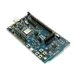
3.1 Hardware content
The nRF52840 Preview Development Kit (DK) contains the development kit board PCA10056 and an NFC
antenna.
Figure 1: nRF52840 Preview DK board (PCA10056) and NFC antenna
3.2 Downloadable content
The nRF52840 Preview DK downloadable content includes the hardware files.
• In the nRF5 SDK, you can find precompiled application firmware examples.
Hardware files
Schematics, layout, bill of materials, and Gerber files for nRF52840 Preview DK are included in a zip file.
• nRF52840 Preview DK hardware files
4440_025 v1.2
7
�Kit content
3.3 Related documentation
In addition to the information in this document, you may need to consult other documents.
Nordic documentation
• nRF52840 Objective Product Specification
• nRF52840 Compatibility Matrix
• nRF52840 Errata
4440_025 v1.2
8
�4
Getting started
Before you start developing, complete a few steps to set up the hardware and download the required
software.
Before you start:
• Unpack the kit.
• Check Minimum requirements on page 6.
Follow the steps below to set up your kit:
1. Connect the NFC antenna to the connector marked NFC.
2. To power up the board:
a) Connect a micro-USB 2.0 cable to the USB connector J2 on the nRF52840 Preview DK and the other
end to one of your PC's USB host port.
In addition to providing power to the board, the USB connection supports target programming.
b) Slide the power switch SW8 to the ON position.
A pop-up may appear. You can ignore it.
Check that LED1 has started pulsating. For more information, see Buttons and LEDs on page 28.
Open Windows Explorer to check that the nRF52840 Preview DK has appeared as a removable drive
named "JLINK".
This allows you to program the chip on the board.
3. Set up the software following the instructions in Nordic tools and downloads in nRF5 Getting Started.
The actual software required depends on your OS and development IDE.
4. To set up a connection between your smart phone and the PDK, enable NFC on your smart phone and
bring your phone close to the PDK.
Your phone will prompt you to open Getting started with the nRF52840 Development Kit. This page
contains a link that makes it easy to install the nRF Toolbox mobile app.
4440_025 v1.2
9
�5
Nordic tools and downloads
Once you have your kit set up you can start developing. Our software tools help you develop and test your
device through all the steps in the software development cycle.
Development IDE
Pick one of the IDEs with a compiler supported by Nordic:
IDE
Windows
Linux
OSX
MDK-ARM Keil µVision
Yes
No
No
GNU/GCC
Yes
Yes
Yes
IAR
Yes
No
No
SEGGER Embedded
Studio (SES)
Yes
Yes
Yes
Essential tools
To program our devices you need to download these Nordic tools.
Tool
Description
Download
Documentation
Protocol
SDK - Software
Development Kit
Application examples,
source files, SoftDevices
Windows/Linux
nRF5 SDK
BLE/ANT
nRF5x Command Line
Tools
Collection of command
line tools, like nrfjprog,
mergehex
nRF5x Tools Windows32
nRF5x
Command
Line Tools
BLE/ANT
nRF5x Tools Linux32
nRF5x Tools Linux64
nRF5x Tools OSX
Optional tools
These tools are not essential, but we recommend that you use them.
4440_025 v1.2
10
�Nordic tools and downloads
Tool
Description
Download
Documentation
Protocol
nRFgo Studio
Programming and
erasing chips
Windows32
Help file
BLE/ANT
Wireless protocol
stack library
Click the Download
tab on:
nRF52 Series SDS
BLE/ANT
SoftDevice
Windows64
nRF52840 Product
page
nRF51 Series SDS
nRF52832 Product
page
nRF51822 Product
page
nRF51422 Product
page
Master Control
Panel
Peer device
emulator for
computers
Windows32
Help file
nRF Connect for
desktop
Peer device
emulator for
computers
nRF Connect for OS- nRF Connect Bluetooth
Low Energy
X
BLE
Windows64
BLE
nRF Connect for
Ubuntu Linux
nRF Connect for
Windows
nRF Connect for
mobile
Peer device
emulator app for
smartphones
Nordic nRF Toolbox
app
App that contains all Android v4.3 or later
the Nordic apps
IOS v8 or later
BLE
Android v4.3 or later
IOS v8 or later
BLE
Windows Phone
v8.1 or later
nRF5x pynrfjprog
A simple Python
interface for the
nrfjprog DLL
nRF5x pynrfjprog
nRF5x pynrfjprog
BLE/ANT
ANTware II
Peer device
emulator for the
ANT protocol
running on
computers
ANTware II
ANTware II
ANT
nRF Sniffer
Monitors on-air
traffic
nRF Sniffer
download
nRF Sniffer
BLE
See also Nordic mobile apps for a list of available Bluetooth Low Energy mobile apps for iOS, Android and
Windows Phones.
4440_025 v1.2
11
�6
Start developing
After you have set up the development kit and installed the toolchain, it is time to start developing.
There are several ways to continue from here. For more information, see the following nRF5 SDK
instructions :
• Running precompiled examples
See how you can quickly test a precompiled example without having to use the full toolchain, it is a
matter of copying and pasting a precompiled HEX file onto your development kit board.
• Compiling and running a first example
Test that you have set up your toolchain correctly by compiling, programming and running a very
simple example.
• Running examples that use a SoftDevice
Before you can run more advanced examples that use Bluetooth or ANT, you must first program the
SoftDevice on the board.
4440_025 v1.2
12
�7
Interface MCU
The interface MCU on the nRF52840 Preview Development Kit (DK) board can run either SEGGER J-Link OB
or mbed OB interface firmware and is used to program and debug the firmware of the nRF52840 SoC.
Figure 2: Interface MCU
7.1 IF Boot/Reset button
The nRF52840 Preview DK board is equipped with an IF Boot/Reset button (SW5).
This button is connected to the interface MCU on the board and has two functions:
• Resetting the nRF52840 SoC.
• Entering bootloader mode of the interface MCU.
During normal operation the button will function as a reset button for the nRF52840 SoC. For this to work,
pin reset on P0.18 needs to be enabled in the SoC.
The button is also used to enter the bootloader mode of the interface MCU. To enter the bootloader
mode, keep the reset button pressed while powering up the board until LED5 starts to blink. You can
power up the board either by disconnecting and reconnecting the USB cable or by toggling the power
switch (SW8).
Note: Pin reset can be enabled by defining the CONFIG_GPIO_AS_PINRESET variable in the
project settings. This can be done, for example, by defining the preprocessor symbol in Keil.
Go to Project > Options for Target > C/C++ > Preprocessor Symbols > Define and add the
CONFIG_GPIO_AS_PINRESET variable after NRF52840_XXAA.
This functionality can be removed by using nrfjprog.exe with arguments --recover -f
NRF52.
7.2 Virtual COM port
The onboard interface MCU features a UART interface through a virtual COM port.
The virtual COM port has the following features:
4440_025 v1.2
13
�Interface MCU
• Flexible baud rate setting up to 1 Mbps.1
• Dynamic hardware flow control (HWFC) handling.
• Tri-stated UART lines when no terminal is connected.
The table below shows an overview of the UART connections on nRF52840 and the interface MCU.
GPIO nRF52840
nRF52840 UART
P0.05
RTS
P0.06
TXD
P0.07
CTS
P0.08
RXD
Table 1: Relationship of UART connections on nRF52840 and interface MCU
The UART signals are routed directly to the interface MCU. The UART pins connected to the interface MCU
are tri-stated when no terminal is connected to the virtual COM port on the computer.
Note: The terminal software used must send a DTR signal to configure the UART interface MCU
pins.
The P0.05 (RTS) and P0.07 (CTS) can be used freely when HWFC is disabled on the SoC.
Note: The mbed OB interface does not support HWFC through the virtual COM port.
7.2.1 Dynamic HWFC handling
When the interface MCU receives a DTR signal from a terminal, it performs automatic hardware flow
control (HWFC) detection.
Automatic HWFC detection is done by driving P0.07 (CTS) from the interface MCU and evaluating the state
of P0.05 (RTS) when the first data is sent or received. If the state of P0.05 (RTS) is high, HWFC is assumed
not to be used. If HWFC is not detected, both CTS and RTS can be used freely by the nRF application.
After a power-on reset of the interface MCU, all UART lines are tri-stated when no terminal is connected
to the virtual COM port. Due to the dynamic HWFC handling, if HWFC has been used and detected, P0.07
(CTS) will be driven by the interface MCU until a power-on reset has been performed or until a new DTR
signal is received and the detection is redone.
To ensure that the UART lines are not affected by the interface MCU, the solder bridges for these signals
can be cut and later resoldered if needed. This might be necessary if UART without HWFC is needed while
P0.05 (RTS) and P0.07 (CTS) are used for other purposes.
7.3 Swapping interface MCU firmware
The onboard interface MCU is factory-programmed with an mbed-compliant bootloader. This feature
makes it possible to swap the interface firmware between the factory-preloaded SEGGER J-Link OB and
the mbed interface firmware.
1. Download the mbed interface firmware and the J-Link OB image from www.nordicsemi.com.
2. Enter the bootloader.
1
Baud rate 921 600 is not supported through the virtual COM port.
4440_025 v1.2
14
�Interface MCU
See section IF Boot/Reset button on page 13 on how to enter the bootloader.
3. To swap the interface MCU firmware, drag the interface image (.bin) into the mounted bootloader
drive on the connected computer.
4. Power cycle the board.
Note:
• The J-Link serial number is linked to the interface MCU and will not change even when swapping
the interface MCU firmware.
• When in bootloader mode, do not drag and drop any files except those downloaded from
www.nordicsemi.com for use with the interface MCU. If a wrong file is used, it can overwrite the
bootloader and ruin the interface MCU firmware without the possibility of recovery.
7.4 MSD
The interface MCU features a mass storage device (MSD). This makes the development kit appear as an
external drive on your computer.
This drive can be used for drag-and-drop programming. However, files cannot be stored on this drive. By
copying a HEX file to the drive, the interface MCU will program the file to the device.
Note:
• Windows might try to defragment the MSD part of the interface MCU. If this happens, the
interface MCU will disconnect and be unresponsive. To return to normal operation, the
development kit must be power cycled.
• Your antivirus software might try to scan the MSD part of the interface MCU. Some antivirus
programs trigger a false positive alert in one of the files and quarantine the unit. If this happens,
the interface MCU will become unresponsive.
• If the computer is set up to boot from USB, it can try to boot from the development kit if the
development kit is connected during boot. This can be avoided by unplugging the development
kit before a computer restart, or changing the boot sequence of the computer.
You can also disable the MSD of the kit by using the msddisable command in J-Link Commander.
To enable, use the msdenable command. These commands take effect after a power cycle of the
development kit and stay this way until changed again.
4440_025 v1.2
15
�8
Hardware description
The nRF52840 Preview Development Kit (DK) board PCA10056 can be used as a development platform for
the nRF52840 SoC. It features an onboard programming and debugging solution.
In addition to radio communication, the nRF52840 SoC can communicate with a computer through USB
and a virtual COM port provided by the interface MCU.
8.1 Hardware drawings
nRF52840 Preview DK hardware drawings show both sides of the PCA10056 board.
Figure 3: nRF52840 Preview DK board front view
Figure 4: nRF52840 Preview DK board back view
8.2 Block diagram
The nRF52840 Preview DK block diagram shows the connections between the different blocks.
4440_025 v1.2
16
�Hardware description
GPIO
LEDs
Buttons
IF Boot/Reset
nRF only mode
switch
Debug out
IF MCU USB
Battery
External supply
External
memory
Matching
network
Interface MCU
Analog switch
Analog switch
Current
measurement
Osc
16 MHz
nRF power
source switch
Osc
32.768 kHz
Li-ion
Debug in
Power supply
circuitry
nRF52840
Power switch
nRF USB
Figure 5: nRF52840 Preview DK block diagram
8.3 Power supply
The nRF52840 Preview DK board has multiple power options.
The power options are:
•
•
•
•
•
•
USB connector J2 for the interface MCU (5 V)
USB connector J3 for the nRF52840 (5 V)
Lithium polymer (Li-Po) battery connectors J6 or P27 (2.5–5.0 V)
VIN 3–5 pin on P20 (3.0–5.0 V)
External supply on P21 (1.7–3.6 V)
Coin cell battery
Figure 6: Power supply options (board front)
4440_025 v1.2
17
Antenna
RF connector
�Hardware description
Figure 7: Power supply options (board back)
8.3.1 5 V power sources
The nRF52840 Preview DK board has a 5 V boost regulator.
It gives a stable 5 V output from four possible sources:
•
•
•
•
USB connector J2 for the interface MCU
USB connector J3 for the nRF52840
Li-Po polymer battery connectors (J6 or P27)
VIN 3–5 V pin on P20
Each of these sources has a reverse protection diode to prevent current flowing in the wrong direction if
multiple sources are connected at the same time.
Figure 8: 5 V regulator and protecting diodes
8.3.2 VDD power sources
The main board supply (VDD) can be sourced from the 5 V domain, external power supply, and coin cell
battery.
For the 5 V domain, there are two regulators, one fixed 3 V buck regulator and one voltage follower
regulator that follows the VDD_nRF voltage. The coin cell battery and external power supply are not
regulated.
• 5 V domain:
• Fixed 3 V buck regulator
• VDD_nRF voltage follower
• External power supply
• Coin cell battery
For more information about power sources, see section nRF52840 power source on page 21.
4440_025 v1.2
18
�Hardware description
The power sources are routed through a set of load switches, which is controlled by logic to give the
correct priority of the power sources.
If the high voltage regulator of the nRF52840 is used, the board will be supplied from the VDD_nRF voltage
follower regardless of the state of the other power sources.
Figure 9: Power supply circuitry
The power switches work in the way that the body diode of the internal transistor powers the VSUPPLY
net, which supplies the gates controlling the enable signal of the switches. If 5 V is present, the switches
4440_025 v1.2
19
�Hardware description
for external supply and battery are disabled. If external supply is present, the switch for the battery is
disabled.
The power switches can be bypassed by shorting one or more solder bridges.
Power source
Power switch bypass
Voltage level
Regulator
SB34
3.0 V
Coin cell battery
SB35
Battery
External supply
SB36
1.7 V–3.6 V
Table 2: Power switch bypass solder bridges
Figure 10: Power switch bypass solder bridges
Note: Connect only one power source at a time. Shorting the solder bridges removes the reverse
voltage protection.
8.3.3 Interface MCU power
The power for the interface MCU is routed through two load switches, one for the VDD supply and one for
the USB supply. This makes it possible to disconnect the interface MCU from the power domain when not
in use.
Figure 11: Interface MCU power switch
4440_025 v1.2
20
�Hardware description
These switches are controlled by the presence of a USB connected to the interface MCU USB connector
(J2), and the state of the nRF only switch (SW6). See section Operating modes on page 22 for more
information.
8.3.4 nRF52840 power source
The nRF52840 Preview DK board has a power source switch (SW9) for selecting between three power
sources for the nRF52840 SoC.
The three positions of the switch are:
• VDD (default)
• Li-Po
• USB
Figure 12: nRF52840 power source switch
The nRF52840 SoC has a high voltage buck regulator that can support up to 5 V input. In the VDD position,
the SoC is powered either from the on-board buck regulator, coin cell battery, or external supply (P21).
In the Li-Po position, the high voltage regulator of the SoC is supplied directly from the Li-Po battery
connectors (J6 or P27). In the USB position, the USB high voltage regulator gets power from the nRF52840
USB connector (J3).
When the high voltage regulator is used, the VDD_nRF voltage can be set by the firmware of the SoC. To
make sure the rest of the board has the same voltage level, the VDD of the board is sourced by a regulator
following the VDD_nRF voltage when the high voltage regulator is used.
Figure 13: VDD_nRF voltage follower and switch
4440_025 v1.2
21
�Hardware description
To make sure that the nRF52840 is not powered when the nRF power switch (SW8) is OFF, two load
switches are used, one for the high voltage regulator (U23) and one for the USB supply (U22). These
switches are controlled by VDD.
8.3.5 nRF52840 direct supply
It is possible to power the SoC directly from a source without powering the rest of the board from the
same source.
The external source can be connected to the external supply connector (P21) and the VEXT->nRF switch
(SW10) put in the ON position. The nRF power source switch (SW9) must be in the VDD position, and the
allowed voltage range is 1.7–3.6 V.
Figure 14: VEXT->nRF switch (SW10)
Since it is only the nRF52840 SoC that is supplied from this source, it is recommended to supply the VDD
domain from a different source (coin cell battery or USB) to prevent the pins of the SoC to be connected to
unpowered devices. To prevent leakage due to voltage differences, the board should be set in the nRF only
mode, see section Operating modes on page 22.
Note: To reduce trace length and parasitic components, the external memory is connected to the
SoC directly instead of using analog switches. It is recommended to cut solder bridges to avoid
leakage, see section External memory on page 25.
8.4 Operating modes
The nRF52840 Preview DK board has various modes of operation.
8.4.1 USB detect
To detect when USB for the interface MCU is connected, there is a circuit sensing the VBUS of USB
connector J2.
When the USB cable is connected, the VDD is propagated to the USB_DETECT signal.
4440_025 v1.2
22
�Hardware description
Figure 15: USB detect
8.4.2 nRF only mode
The nRF only mode disconnects the interface MCU and LEDs from the SoC using analog switches.
This is done to isolate the chip on the board as much as possible, and can be of use when measuring
currents on low-power applications.
Figure 16: nRF only switch (SW6)
8.4.3 Signal switches
On the nRF52840 Preview DK board, there are multiple analog switches that are used to connect and
disconnect signals based on different scenarios.
4440_025 v1.2
23
�Hardware description
Figure 17: Signal switches
The USB and SW6 control the signal switches by using USB_DETECT as an input to SW6. Therefore, the
interface MCU can be disconnected either by unplugging the USB cable in J2 or by toggling SW6.
The signal controls a set of switches (U5, U6, U7) that break the connection between the nRF52840 and
the interface MCU, and control the power for the interface MCU. For more information, see section
Interface MCU power on page 20.
Switches U5 and U6 break the connection of the UART lines and SWD/RESET lines. In addition, the
signal controls the routing of the RESET signal depending on user preference when the interface MCU is
connected/disconnected.
• When the interface MCU is disconnected, cutting SB42 will disconnect the IF Boot/Reset button from
the reset pin (P0.18) of nRF52840.
• When the interface MCU is disconnected, shorting SB45 will connect the RESET pin in the Arduino
interface to the reset pin (P0.18) of nRF52840.
4440_025 v1.2
24
�Hardware description
• When the interface MCU is connected, shorting SB46 will connect the RESET pin in the Arduino
interface to the BOOT input of the interface MCU.
• Shorting SB43 will connect the RESET pin in the Arduino interface to the IF Boot/Reset button.
• Shorting SB44 will connect the RESET pin in the Arduino interface to the reset pin (P0.18) of nRF52840.
When a shield is connected, there are two analog switches connecting the pull-up resistors to the I2C bus
lines (SDA and SCL). This function is using one ground pin on the Arduino shield to control the switch. This
feature can be disabled by cutting SB33. To permanently enable pull-up resistors, short SB32.
Figure 18: Solder bridges: Shield detect and reset behavior
The last switch (U8) controls which GPIOs certain signals are routed to. This is due to some features using
the same GPIOs as the Trace output by default. These analog switches are controlled by SW7. See chapter
Debug input and trace on page 34 for more information.
8.5 External memory
The nRF52840 Preview DK board has a 64 Mb external flash memory. The memory is a multi-I/O memory
supporting both regular SPI and Quad SPI.
The memory is connected to the chip using the following GPIOs:
GPIO
Flash memory pin
Solder bridge for
memory use (default:
shorted)
Solder bridge for GPIO
use (default: open)
P0.17
CS
SB13
SB23
P0.19
SCLK
SB11
SB21
P0.20
SIO_0/SI
SB12
SB22
P0.21
SIO_1/SO
SB14
SB24
P0.22
SIO_2/WP
SB15
SB25
P023
SIO_3/HOLD
SB10
SB20
Table 3: Flash memory GPIO usage and connecting solder bridges
To use the GPIOs for a purpose other than the onboard external memory and have them available on the
P24 connector, six solder bridges (SB10–SB15) must be cut and six solder bridges (SB20–SB25) must be
shorted. See Figure 19: Configuring GPIOs for external memory on page 26 for details.
4440_025 v1.2
25
�Hardware description
Note: If debugging the QSPI communication is needed, the SB20–SB25 can be shorted without
cutting SB10–SB15, but the pins should not be driven externally.
Figure 19: Configuring GPIOs for external memory
By default, the power supply of the external memory is coming from the VDD domain and it is controlled
by the nRF only switch (SW6). In the nRF only mode, there are two optional power sources for keeping
the external memory powered, VDD and VDD_nRF. If VDD_nRF is selected, the power consumption of the
external memory will be added to the nRF52840 current measured on P22 or P23. See the following table
for configuration:
Power source
Solder bridge
Default state
VDD_PER
SB16
Shorted
VDD
SB17
Open
VDD_nRF
SB18
Open
Table 4: Flash memory power source configuration
8.6 Connector interface
Access to the nRF52840 GPIOs is available from connectors P2, P3, P4, P5, P6, and P24.
The P1 connector provides access to ground and power on the nRF52840 Preview DK board.
4440_025 v1.2
26
�Hardware description
Figure 20: nRF52840 Preview DK board connectors
Some of the signals are also available on connectors P7, P8, P9, P10, P11, and P12, which are on the
bottom side of the board. By mounting pin lists on the connector footprints, the nRF52840 Preview
DK board can be used as a shield for Arduino motherboards2 or other boards that follow the Arduino
standard.
For easy access to GPIO, power, and ground, the signals can also be found on the through-hole connectors
P13–P17.
Note:
Some pins have default settings:
• P0.00 and P0.01 are used for the 32.768 kHz crystal and are not available on the connectors. For
more information, see section 32.768 kHz crystal on page 29.
• P0.05, P0.06, P0.07, and P0.08 are used by the UART connected to the interface MCU. For more
information, see section Virtual COM port on page 13.
• P0.09 and P0.10 are by default used by NFC1 and NFC2. For more information, see section NFC
antenna interface on page 36.
• P0.11–P0.16 and P0.24–P0.25 are by default connected to the buttons and LEDs. For more
information, see section Buttons and LEDs on page 28.
• P0.17 and P0.19–P0.23 are by default connected to the external memory. For more information,
see section External memory on page 25.
2
Only 3.3 V Arduino boards.
4440_025 v1.2
27
�Hardware description
When the nRF52840 Preview DK board is used as a shield together with an Arduino standard
motherboard, the Arduino signals are routed as shown in the figure below.
Figure 21: Arduino signals routing on the nRF52840 Preview DK board
8.7 Buttons and LEDs
The four buttons and four LEDs on the nRF52840 Preview DK board are connected to dedicated GPIOs on
the nRF52840 chip.
Part
GPIO
GPIO alternative
Solder bridge
Button 1
P0.11
P1.07
-
Button 2
P0.12
P1.08
-
Button 3
P0.24
-
Button 4
P0.25
-
LED 1
P0.13
SB5
LED 2
P0.14
SB6
LED 3
P0.15
SB7
LED 4
P0.16
SB8
Table 5: Button and LED connection
4440_025 v1.2
28
�Hardware description
If P0.13–P0.16 are needed elsewhere, the LEDs can be disconnected by cutting the short on SB5–SB8, see
figure Figure 22: Disconnecting the LEDs on page 29. Since P0.11 and P0.12 are used as a part of the
Trace functionality, Button 1 and Button 2 can be moved to alternative GPIOs, see chapter Debug input
and trace on page 34 for more information.
Figure 22: Disconnecting the LEDs
The buttons are active low, meaning that the input will be connected to ground when the button is
activated. The buttons have no external pull-up resistor, and therefore, to use the buttons, the P0.11,
P0.12, P0.24, P0.25 pins must be configured as an input with an internal pull-up resistor.
The LEDs are active low, meaning that writing a logical zero ('0') to the output pin will illuminate the LED.
Figure 23: Button and LED configuration
8.8 32.768 kHz crystal
The nRF52840 SoC can use an optional 32.768 kHz crystal (X2) for higher accuracy and lower average
power consumption.
On the nRF52840 Preview DK board, P0.00 and P0.01 are by default used for the 32.768 kHz crystal and
are not available as GPIO on the connectors.
Note: When using ANT/ANT+, the 32.768 kHz crystal (X2) is required for correct operation.
If P0.00 and P0.01 are needed as normal I/Os, the 32.768 kHz crystal can be disconnected and the
GPIO routed to the connectors. Cut the shorting track on SB1 and SB2, and solder SB3 and SB4. See the
following figure for reference.
4440_025 v1.2
29
�Hardware description
Figure 24: Configuring P0.00 and P0.01
Figure 25: 32.768 kHz crystal and SB1–SB4 schematic
8.9 Measuring current
The current drawn by the nRF52840 SoC can be monitored on the nRF52840 Preview DK board.
There are several types of test equipment that can be used to measure current, and each type has some
advantages and some disadvantages. The test equipment types are:
•
•
•
•
Power analyzer
Oscilloscope
Ampere-meter
Power Profiler Kit
Power analyzer and Power Profiler Kit measurements will not be described in the present document. For
more information on Power Profiler Kit, see Power Profiler Kit User Guide.
For instructions for measuring, see sections Using an oscilloscope for current profile measurement on
page 31 and Using an ampere-meter for current measurement on page 32.
The nRF52840 SoC has two possible power supplies, VDD (1.7–3.6 V) and VDDH (2.5–5.5 V). The
nRF52840 Preview DK is prepared for measuring current on both domains. Only the VDD domain current
measurement is described here, but the approach is the same with the VDDH supply. See the following
table for the corresponding components:
4440_025 v1.2
30
�Hardware description
Component
VDD
VDDH
Measurement connector
P22
P23
Solder bridge
SB40
SB41
Series resistor
R90
R91
Table 6: Components for current measurement on VDD and VDDH
Note: When measuring the current consumption:
• It is not recommended to use a USB connector to power the board during current
measurements. However, when measuring current on an application using the USB interface of
the nRF52840 SoC, the USB must be connected. It is recommended to power the board from
a coin cell battery, external power supply on connector P21 (1.7–3.6 V), or through the Li-Po
connector J6 or P27 (2.5–5.0 V).
• The current measurements will become unreliable when a serial terminal is connected to the
virtual COM port.
• After programming the nRF52840 SoC, the USB for the interface MCU must be disconnected.
For more information on current measurement, see the tutorial Current measurement guide:
Introduction.
8.9.1 Preparing the development kit board
To measure current, you must first prepare the board.
The suggested configurations actually split the power domains for the nRF52840 SoC and the rest of the
board.
Figure 26: Prepare the development kit board for current measurements
• To put P22 in series with the load, cut the PCB track shorting solder bridge SB40.
• To restore normal kit function after measurement, solder SB9 or apply a jumper on P22.
• To reprogram the nRF52840 SoC while the board is prepared for current measurements, remove
measurement devices from P22, and then connect the USB cable.
8.9.2 Using an oscilloscope for current profile measurement
An oscilloscope can be used to measure both the average current over a given time interval and capture
the current profile.
4440_025 v1.2
31
�Hardware description
Make sure you have prepared the development kit board as described in section Preparing the
development kit board on page 31.
1. Mount a 10 Ω resistor on the footprint for R90.
2. Connect an oscilloscope in differential mode or similar with two probes on the pins of the P22
connector as shown in Figure 27: Current measurement with oscilloscope on page 32.
3. Calculate or plot the instantaneous current from the voltage drop across the 10 Ω resistor by taking the
difference of the voltages measured on the two probes. The voltage drop will be proportional to the
current. The 10 Ω resistor will cause a 10 mV drop for each 1 mA drawn by the circuit being measured.
The plotted voltage drop can be used to calculate the current at a given point in time. The current can
then be averaged or integrated to analyze current and energy consumption over a period.
Figure 27: Current measurement with oscilloscope
Some tips to reduce noise:
• Use probes with 1× attenuation
• Enable averaging mode to reduce random noise
• Enable high resolution function if available
Use a minimum of 200 kSa/s (one sample every 5 µs) to get the correct average current measurement.
8.9.3 Using an ampere-meter for current measurement
The average current drawn by the nRF52840 SoC can be measured using an ampere-meter. This method
will monitor the current in series with the nRF device.
Make sure you have prepared the development kit board as described in section Preparing the
development kit board on page 31.
Connect an ampere-meter between the pins of connector P22 as shown in the figure below.
4440_025 v1.2
32
�Hardware description
Figure 28: Current measurement with an ampere-meter
Note: An ampere-meter will measure the average current drawn by the nRF52840 SoC if:
• The SoC is in a state where it draws a constant current, or, the activity on the device changing
load current, like BLE connection events, is repeated continuously and has a short cycle time
(less than 100 ms) so that the ampere-meter will average whole load cycles and not parts of the
cycle.
• The dynamic range of the ampere-meter is wide enough to give accurate measurements from 1
µA to 15 mA.
• Recommendation: Use a true RMS ampere-meter.
8.10 RF measurements
The nRF52840 Preview DK board is equipped with a small coaxial connector (J1) for conducting
measurements of the RF signal using a spectrum analyzer.
The connector is of SWF type (Murata part no. MM8130-2600) with an internal switch. By default, when
no cable is attached, the RF signal is routed to the onboard trace antenna.
A test probe is available (Murata part no. MXHS83QE3000) with a standard SMA connection on the other
end for connecting instruments (the test probe is not included with the kit). When connecting the test
probe, the internal switch in the SWF connector will disconnect the onboard antenna and connect the RF
signal from the nRF52840 SoC to the test probe.
4440_025 v1.2
33
�Hardware description
Figure 29: Connecting a spectrum analyzer
The connector and test probe will add loss to the RF signal, which should be taken into account when
measuring, see the following table:
Frequency (MHz)
Loss (dB)
2440
1.0
4880
1.7
7320
2.6
Table 7: Typical loss in connector and test probe
8.11 Debug input and trace
The Debug in connector (P18) makes it possible to connect external debuggers for debugging when the
interface MCU USB cable is not connected or the board is in nRF only mode.
Figure 30: Debug input and TRACE connectors
4440_025 v1.2
34
�Hardware description
For trace, a footprint for a 20-pin connector is available (P25). If trace functionality is required, a 2×10 pin
1.27 mm pitch surface mount pin header can be mounted.
Some of the trace pins are by default used for other functionality on the board. By sliding the TRACE
switch (SW7) from Def. to Alt., the functionality is moved to other GPIOs. See the following table:
GPIO
Trace
Default use
Optional GPIO
P0.07
TRACECLK
UART CTS
P0.04
P1.00
TRACEDATA[0]
P0.11
TRACEDATA[1]
Button 1
P1.07
P0.12
TRACEDATA[2]
Button 2
P1.08
P1.09
TRACEDATA[3]
Table 8: Default and Trace GPIOs
8.12 Debug output
The nRF52840 Preview DK board supports programming and debugging external boards with nRF51 or
nRF52 SoCs. To debug an external board with SEGGER J-Link OB IF, connect to the Debug out connector
(P19) with a 10-pin cable.
Figure 31: Debug output connector
When the external board is powered, the interface MCU will detect the supply voltage of the board and
program/debug the target chip on the external board instead of the onboard nRF52840 SoC.
Note: The voltage supported by external debugging/programming is VDD voltage. Normally, this
is 3 V when running from USB, but if the onboard nRF52840 SoC is supplied from either USB or LiIon, the nRF power source switch (SW9) is in either Li-Po or USB position, and VDD can be set by
the nRF52840 firmware. Make sure the voltage level of the external board matches the VDD of the
nRF52840 Preview DK.
You can also use P20 as a debug out connection to program shield-mounted targets. For both P19 and
P20, the interface MCU will detect the supply voltage on the mounted shield and program/debug the
target.
If the interface MCU detects target power on both P19 and P20, it will by default program/debug the
target connected to P19.
4440_025 v1.2
35
�Hardware description
If it is inconvenient to have a separate power supply on the external board, the nRF52840 Preview DK
board can supply power through the Debug out connector (P19). To enable this, short solder bridge SB47.
Note that as long as SB47 is shorted, it is not possible to program the onboard nRF52840 SoC even if the
external board is unplugged.
8.13 NFC antenna interface
The nRF52840 Preview DK board supports a near field communication (NFC) tag.
NFC-A listen mode operation is supported on the nRF52840 SoC. The NFC antenna input is available on
connector J5 on the nRF52840 Preview DK board.
Figure 32: NFC antenna connector
NFC uses two pins, L24 (NFC1) and J24 (NFC2), to connect the antenna. These pins are shared with GPIOs
(P0.09 and P0.10) and the PROTECT field in the NFCPINS register in UICR defines the usage of these pins
and their protection level against abnormal voltages. The content of the NFCPINS register is reloaded at
every reset.
Note: The NFC pins are enabled by default.
NFC can be disabled and GPIOs enabled by defining the CONFIG_NFCT_PINS_AS_GPIOS variable in the
project settings. This can be done by defining the preprocessor symbol in Keil. Go to Project > Options
for Target > C/C++ > Preprocessor Symbols > Define and add the CONFIG_NFCT_PINS_AS_GPIOS variable
after NRF52.
This functionality can be removed by using nrfjprog.exe with arguments --recover -f NRF52.
Pins L24 and J24 are by default configured to use the NFC antenna, but if they are needed as normal
GPIOs, R44 and R46 must be NC and R43 and R45 must be shorted by 0R.
Figure 33: NFC input schematic
4440_025 v1.2
36
�Hardware description
8.14 Extra op-amp
The voltage follower for the power supply uses a dual package op-amp.
The extra op-amp has been routed out to a connector (P28, not mounted) so that it is accessible for the
user.
For more information on the power supply, see section nRF52840 power source on page 21.
Figure 34: Extra op-amp
8.15 Solder bridge configuration
This complete overview of solder bridges on the nRF52840 Preview DK helps to change the default state.
Solderbridge
Default
Function
SB1
Closed
Cut to disconnect the 32.768 kHz on P0.01
SB2
Closed
Cut to disconnect the 32.768 kHz on P0.00
SB3
Open
Short to enable P0.01 as normal GPIO
SB4
Open
Short to enable P0.00 as normal GPIO
SB5
Closed
Cut to disconnect LED1
SB6
Closed
Cut to disconnect LED2
SB7
Closed
Cut to disconnect LED3
SB8
Closed
Cut to disconnect LED4
SB9
Open
Short to bypass peripheral power switch
SB10
Closed
Cut to disconnect the QSPI memory from P0.23
SB11
Closed
Cut to disconnect the QSPI memory from P0.19
SB12
Closed
Cut to disconnect the QSPI memory from P0.20
SB13
Closed
Cut to disconnect the QSPI memory from P0.17
SB14
Closed
Cut to disconnect the QSPI memory from P0.21
SB15
Closed
Cut to disconnect the QSPI memory from P0.22
SB16
Closed
Cut to disconnect QSPI memory power supply from VDD_PER
SB17
Open
Short to connect QSPI memory power supply to VDD
SB18
Open
Short to connect QSPI memory power supply to VDD_nRF
SB20
Open
Short to enable P0.23 as a normal GPIO
SB21
Open
Short to enable P0.19 as a normal GPIO
4440_025 v1.2
37
�Hardware description
Solderbridge
Default
Function
SB22
Open
Short to enable P0.20 as a normal GPIO
SB23
Open
Short to enable P0.17 as a normal GPIO
SB24
Open
Short to enable P0.21 as a normal GPIO
SB25
Open
Short to enable P0.22 as a normal GPIO
SB30
Open
Short to reset the interface MCU
SB31
Open
Short to bypass the USB detect switch
SB32
Open
Short to permanently enable the I2C pull-up resistors
SB33
Closed
Cut to permanently disable the I2C pull-up resistors
SB34
Open
Short to bypass the power switch on the USB power
SB35
Open
Short to bypass the power switch on the coin cell battery power
SB36
Open
Short to bypass the power switch on the external supply power
SB37
Open
Short to bypass the interface MCU power switch
SB38
Closed
Cut to disable VDD power to the Arduino interface
SB39
Open
Short to bypass the power switch for regulator, coin cell, or external
supply
SB40
Closed
Cut for current measurements of the VDD_nRF
SB41
Closed
Cut for current measurements of the VDD_nRF_HV
SB42
Closed
Cut to disconnect IF Boot/Reset button from nRF52840 reset pin
when the interface MCU is disconnected
SB43
Open
Short to connect IF Boot/Reset button to RESET pin on the Arduino
interface
SB44
Open
Short to connect the RESET pin on the Arduino interface to the
nRF52840 reset pin
SB45
Open
Short to connect the RESET pin on the Arduino interface to
the interface nRF52840 reset pin when the interface MCU is
disconnected
SB46
Open
Short to connect the RESET pin on the Arduino interface to the
interface MCU Boot when the interface MCU is disconnected
SB47
Open
Short to enable power supply of the external device when using the
debug out connector
SB48
Open
Short to bypass the interface MCU USB power switch
SB49
Open
Short to connect VDD_UTMI to VDD_SAM
SB50
Closed
Cut to disconnect the nRF52840 CTS line from the signal switch and
interface MCU
SB51
Closed
Cut to disconnect the nRF52840 RTS line from the signal switch and
interface MCU
SB52
Closed
Cut to disconnect the nRF52840 RxD line from the signal switch and
the interface MCU
4440_025 v1.2
38
�Hardware description
Solderbridge
Default
Function
SB53
Closed
Cut to disconnect the nRF52840 TxD line from the signal switch and
interface MCU
SB54
Closed
Cut to disconnect the nRF52840 SWDIO line from the signal switch
and interface MCU
SB55
Closed
Cut to disconnect the nRF52840 SWDCLK line from the signal switch
and interface MCU
SB56
Closed
Cut to disconnect the nRF52840 RESET line from the signal switch
and interface MCU
SB57
Closed
Cut to disconnect the nRF52840 SWO line from the signal switch and
the interface MCU
SB65
Closed
Cut to disable the pull-up resistor of the IMCU_BOOT line
SB80
Open
Short to bypass the power switch for the VBUS of nRF52840
SB81
Open
Short to bypass the power switch for VDD_HV of nRF52840
Table 9: Solder bridge configuration
4440_025 v1.2
39
�Legal notices
By using this documentation you agree to our terms and conditions of use. Nordic Semiconductor may
change these terms and conditions at any time without notice.
Liability disclaimer
Nordic Semiconductor ASA reserves the right to make changes without further notice to the product to
improve reliability, function or design. Nordic Semiconductor ASA does not assume any liability arising out
of the application or use of any product or circuits described herein.
All information contained in this document represents information on the product at the time of
publication. Nordic Semiconductor ASA reserves the right to make corrections, enhancements, and other
changes to this document without notice. While Nordic Semiconductor ASA has used reasonable care
in preparing the information included in this document, it may contain technical or other inaccuracies,
omissions and typographical errors. Nordic Semiconductor ASA assumes no liability whatsoever for any
damages incurred by you resulting from errors in or omissions from the information included herein.
Life support applications
Nordic Semiconductor products are not designed for use in life support appliances, devices, or systems
where malfunction of these products can reasonably be expected to result in personal injury.
Nordic Semiconductor ASA customers using or selling these products for use in such applications do so
at their own risk and agree to fully indemnify Nordic Semiconductor ASA for any damages resulting from
such improper use or sale.
RoHS and REACH statement
Nordic Semiconductor products meet the requirements of Directive 2011/65/EU of the European
Parliament and of the Council on the Restriction of Hazardous Substances (RoHS 2) and the requirements
of the REACH regulation (EC 1907/2006) on Registration, Evaluation, Authorization and Restriction of
Chemicals.
The SVHC (Substances of Very High Concern) candidate list is continually being updated. Complete
hazardous substance reports, material composition reports and latest version of Nordic's REACH
statement can be found on our website www.nordicsemi.com.
Trademarks
All trademarks, service marks, trade names, product names and logos appearing in this documentation are
the property of their respective owners.
Copyright notice
© 2017 Nordic Semiconductor ASA. All rights are reserved. Reproduction in whole or in part is prohibited
without the prior written permission of the copyright holder.
4440_025 v1.2
40
�