TS5204
Taiwan Semiconductor
80mA Low Noise Ultra Low Dropout Voltage Regulator
DESCRIPTION
FEATURES
The TS5204 series is an efficient linear voltage
regulator with ultra-low noise output, very low dropout
voltage (typically 20mV at light loads and 300mV at
80mA), and very low power consumption (500µA at
50mA), providing high output current even when the
application requires very low dropout voltage. The
TS5204 series is included a precision voltage reference,
error correction circuit, a current limited output driver,
over temperature shutdown and revered battery
protection.
●
Ultra-Low Noise Output
●
Output Current up to 80mA
●
Low Dropout Voltage
●
Low Power Consumption
●
●
●
Internal Current Limit
Thermal Shutdown Protection
Compliant to RoHS Directive 2011/65/EU and in
accordance to WEEE 2002/96/EC.
Halogen-free according to IEC 61249-2-21
●
APPLICATION
SOT-23
Pin Definition:
1. Output
2. Input
3. Ground
●
Cellular Telephones
●
Palmtops, Notebook Computers
●
Battery Powered Equipment
●
Consumer and Personal Electronics
●
SMPS Post Regulator and DC to DC Modules
●
High-efficiency Linear Power Supplies
●
Portable Application
Pin Definition:
1. Output
2. Ground
3. Input
SOT-89
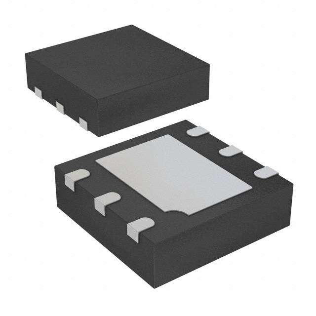
DFN2x2
Pin Definition:
1. Output
2. N/C
3. Ground
4. N/C
5. N/C
6. Output
TYPICAL APPLICATION CIRCUIT
1
Version: L1609
�TS5204
Taiwan Semiconductor
ABSOLUTE MAXIMUM RATINGS (TA = 25°C unless otherwise noted) (Note 1)
PARAMETER
SYMBOL
LIMIT
UNIT
Input Supply Voltage
VIN
-20~ +20
V
Recommend Operating Input Voltage
VIN
+2.5 ~ +16
V
PD
Internal limited
Io
80
Power Dissipation
(Note 2)
Output Current
SOT-23
Junction to Ambient Thermal Resistance
mA
220
SOT-89
180
RӨJA
DFN2x2
°C/W
80
Operating Junction Temperature Range
Storage Temperature Range
TJ
-40 ~ +150
°C
TSTG
-65 ~ +150
°C
Notes:
1. Exceeding the absolute maximum rating may damage the device.
2. The maximum allowable power dissipation at any TA is PD(MAX) = [TJ(MAX) - Ta] + RӨJA. Exceeding the maximum allowable
power dissipation will result in excessive die temperature, and the regulator will go into thermal shutdown.
3. The device is not guaranteed to function outside its operating rating.
ELECTRICAL SPECIFICATIONS (TA = 25°C unless otherwise noted)
PARAMETER
CONDITIONS
Output Voltage
Output Voltage Temp. Coefficient
MIN
VIN=VO + 1V
0.97|Vo|
VIN=VO + 1V, IO= 80mA
0.96|Vo|
(Note 3)
TYP
VOUT
MAX
1.03|Vo|
1.04|Vo|
UNIT
V
--
50
--
ppm/°C
VO+1V ≤ VIN ≤ 16V
--
0.1
0.5
%
0.1mA ≤ IO ≤ 80mA
--
1
2
%
IO=100μA
--
20
--
IO=50mA
--
250
400
IO=80mA
--
300
600
IO=100μA
--
180
--
IO=50mA
--
850
1250
IO=80mA
--
2600
3100
Output Current Limit
VOUT=0V
--
180
--
mA
Power Supply Rejection Ratio
At f=100Hz, IO=100μA,
--
65
--
dB
--
0.05
--
%/W
--
260
--
nV√Hz
Line Regulation
Load Regulation
(Note 4)
Dropout Voltage
(Note 6)
Ground Pin Current
Thermal Regulation
Output Noise
(Note 7)
(Note 8)
IO=50mA,
COUT =2.2μF,
mV
μA
Note:
4. Output voltage temperature coefficient is defined as the worst case voltage change divided by the total temperature range.
5. Regulation is measured at constant junction temperature using low duty cycle pulse testing. Parts are tested for load
regulation in the load range from 1mA to 80mA. Changes in output voltage due to heating effects are covered by the thermal
regulation specification.
6. Dropout voltage is defined as the input to output differential at which the output voltage drops 2% below its nominal value
measured at 1V differential.
7. Ground pin current is the regulator quiescent current plus pass transistor base current. The total current drawn from the
supply is the sum of the load current plus the ground pin current.
8. Thermal regulation is defined as the change in output voltage at a time “t” after a change in power dissipation is applied,
excluding load or line regulation effects. Specifications are for a 80mA load pulse at VIN =16V for t=10ms.
2
Version: L1609
�TS5204
Taiwan Semiconductor
ORDERING INFORMATION
OUTPUT VOLTAGE
PART NO.
3.3V
5V
PACKAGE
PACKING
TS5204CQ33 RFG
DFN2x2
3,000pcs / 7” Reel
TS5204CX33 RFG
SOT-23
3,000pcs / 7” Reel
TS5204CY50 RMG
SOT-89
1,000pcs / 7” Reel
TS5204CX50 RFG
SOT-23
3,000pcs / 7” Reel
APPLICATION INFORMATION
TS5204 series is designed to provide 80mA of continuous current in a very small package. Maximum power
dissipation can be calculated based on the output current and the voltage drop across the part. To determine the
maximum power dissipation of the package, use the junction-ambient thermal resistance of the device and the
following basic equation:
PD(MAX) = [ TJ(MAX) – TA ] /RΘJA
Tj(max) is the maximum junction temperature of the die(125°C), and Ta is the ambient operating temperature.
RΘJA is layout dependent, the actual power dissipation of the regulator circuit can be determined using the
equation:
PD = (VIN – VOUT) * IOUT + VIN * IGND
Substituting PD(MAX) for PD and solving for the operating conditions that are critical to the application will give the
maximum operating conditions for the regulator circuit. For example, when operating the TS5204CX33 at room
temperature with a minimum footprint layout, the maximum input voltage for a set output current can be
determined as follows:
o
o
o
PD(MAX) = (125 C – 25 C) / 220 C/W
The junction to ambient thermal resistance for the minimum footprint is 220°C/W, the maximum power dissipation
must not be exceeded for proper operation. Using the output voltage of 3.3V and an output current of 80mA, the
maximum input voltage can be determined. From the electrical characteristics table, the maximum ground
current for 80mA output current is 2.5mA.
445mW = (VIN – 3.3V ) * 120mA + VIN * 2.5mA
445mW = VIN * 120mA – 3.3 * 120mA + VIN * 2.5mA
445mW = VIN * 120mA – 395mW + VIN * 2.5mA
840mW = VIN * 122.5mA
VIN (max) = 6.85V
Therefore, a 3.3V application at 80mA of output current can accept a maximum input voltage of 6.85V in a SOT23 package.
Input Capacitor Requirement
An input capacitor of 0.1μF or greater is recommended when the device is more than 10” away from the bulk AC
supply capacitance or when the supply is a battery.
3
Version: L1609
�TS5204
Taiwan Semiconductor
APPLICATION INFORMATION (CONTINUE)
Output Capacitor Requirement
The TS5204 series requires an output capacitor to maintain stability and improve transient response is necessary.
2.2μF minimum is recommended. Larger values improve the regulator’s transient response. The output capacitor
value may be increased without limit.
The output capacitor should have an ESR (effective series resistance) less than 5Ω and a resonant frequency
above 1MHz. Ultra-low ESR capacitors can cause a low amplitude oscillation on the output and/or under damped
transient response. Most of tantalum or aluminum electrolytic capacitors are adequate; film types will work. Since
many aluminum electrolytic have electrolytes that freeze at about –30°C, solid tantalums are recommended for
operation below –25°C. At lower values of output current, less output capacitance is required for output stability.
The capacitor can be reduced to 0.47μF for current below 10mA or 0.33μF for currents below 1mA.
No Load Stability
The TS5204 series will remain stable and in regulation with no load, unlike many other voltage regulators. This is
especially important in CMOS RAM keep alive applications.
Dual Supply Operation
When used in dual supply systems where the regulator load is returned to a negative supply, the output voltage
must be diode clamped to ground.
ELECTRICAL CHARACTERICS CURVES (TA=25oC, unless otherwise noted)
Figure 1. Dropout Voltage vs. Output Current
Figure 2. Ground Current vs. Output Current
Figure 3. Dropout Voltage vs. Output Current
Figure 4. Short Circuit Current vs. Input Voltage
4
Version: L1609
�TS5204
Taiwan Semiconductor
PACKAGE OUTLINE DIMENSIONS (Unit: Millimeters)
SOT-23
SUGGESTED PAD LAYOUT (Unit: Millimeters)
MARKING DIAGRAM
= Device Code
= Voltage Code
(5 = 5.0V, S = 3.3V)
Y = Year Code
M = Month Code for Halogen Free Product
O =Jan P =Feb Q =Mar R =Apr
S =May T =Jun U =Jul
V =Aug
W =Sep X =Oct
Y =Nov Z =Dec
L = Lot Code
J
x
5
Version: L1609
�TS5204
Taiwan Semiconductor
PACKAGE OUTLINE DIMENSIONS (Unit: Millimeters)
SOT-89
SUGGESTED PAD LAYOUT (Unit: Millimeters)
MARKING DIAGRAM
= Year Code
= Month Code for Halogen Free Product
O =Jan P =Feb Q =Mar R =Apr
S =May T =Jun U =Jul
V =Aug
W =Sep X =Oct
Y =Nov Z =Dec
L = Lot Code
xx = Voltage
(50 = 5.0V)
Y
M
6
Version: L1609
�TS5204
Taiwan Semiconductor
PACKAGE OUTLINE DIMENSIONS (Unit: Millimeters)
DFN2x2
SUGGESTED PAD LAYOUT (Unit: Millimeters)
MARKING DIAGRAM
= Device Code
= Fixed Output Voltage Code
(33 =3.3V)
Y = Year Code
M = Month Code for Halogen Free Product
O =Jan P =Feb Q =Mar R =Apr
S =May T =Jun U =Jul
V =Aug
W =Sep X =Oct
Y =Nov Z =Dec
L = Lot Code
J
xx
7
Version: L1609
�TS5204
Taiwan Semiconductor
Notice
Specifications of the products displayed herein are subject to change without notice. TSC or anyone on its behalf,
assumes no responsibility or liability for any errors or inaccuracies.
Information contained herein is intended to provide a product description only. No license, express or implied, to
any intellectual property rights is granted by this document. Except as provided in TSC’s terms and conditions of
sale for such products, TSC assumes no liability whatsoever, and disclaims any express or implied warranty,
relating to sale and/or use of TSC products including liability or warranties relating to fitness for a particular purpose,
merchantability, or infringement of any patent, copyright, or other intellectual property right.
The products shown herein are not designed for use in medical, life-saving, or life-sustaining applications.
Customers using or selling these products for use in such applications do so at their own risk and agree to fully
indemnify TSC for any damages resulting from such improper use or sale.
8
Version: L1609
�
很抱歉,暂时无法提供与“TS5204CQ33 RFG”相匹配的价格&库存,您可以联系我们找货
免费人工找货