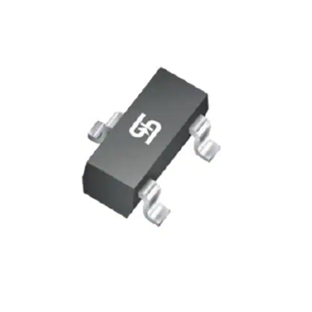
TS9011
Taiwan Semiconductor
250mA Low Quiescent Current CMOS LDO
DESCRIPTION
FEATURES
TS9011 is a positive voltage regulator developed
●
Dropout Voltage 0.4V (typ.) @ Io=250mA
utilizing CMOS technology featured very low power
●
Output Current up to 250mA
consumption, low dropout voltage and high output
●
Low Power Consumption, 2µA (typ.)
voltage accuracy. Built in low on-resistor provides
●
Output Voltage ± 2%
low dropout voltage and large output current. A 1µF
●
Internal Current Limit
or greater can be used as an output capacitor.
●
●
Thermal Shutdown Protection
Compliant to RoHS Directive 2011/65/EU and in
accordance to WEEE 2002/96/EC.
Halogen-free according to IEC 61249-2-21
TS9011 are prevented device failure under the worst
operation condition with both thermal shutdown and
●
current fold-back. These series are recommended for
configuring portable devices and large current
APPLICATION
application, respectively.
●
Battery-operated systems
●
Microprocessor reset circuitry
●
Memory battery back-up circuits
●
Power-on reset circuits
●
Power failure detection
●
System battery life and charge voltage monitors
SOT-23
SOT-89
Pin Definition:
1. Ground
2. Output
3. Input
Pin Definition:
1. Ground
2. Input
3. Output
Notes: Moisture sensitivity level: level 3. Per J-STD-020
TYPICAL APPLICATION CIRCUIT
*Tantalum capacitor for Input & Output capacitor are recommended.
1
Version: H1608
�TS9011
Taiwan Semiconductor
ABSOLUTE MAXIMUM RATINGS (TA = 25°C unless otherwise specified) (Note 1)
PARAMETER
SYMBOL
LIMIT
UNIT
VIN
IOUT
V
mA
TOPR
TJ
TSTG
12
250
0.30
0.50
-40 ~ +85
-40 ~ +150
-65 ~ +150
SYMBOL
LIMIT
UNIT
Input Supply Voltage
Output Current
SOT-23
SOT-89
Power Dissipation
PD
Operating Ambient Temperature
Junction Temperature Range
Storage Temperature Range
W
o
C
C
o
C
o
THERMAL PERFORMANCE
PARAMETER
SOT-23
Thermal Resistance - Junction to Ambient
SOT-89
333
RӨJA
o
C/W
200
Note: Measured with FR4 4-layer board having thermal via holes
ELECTRICAL SPECIFICATIONS (TA = 25°C unless otherwise specified)
PARAMETER
CONDITION
TS90115
MIN
TYP
MAX
4.90
5.0
5.10
TS9011S
3.23
3.3
3.36
TS9011P
2.94
3.0
3.06
TS9011K
2.45
2.5
2.55
TS9011D
1.76
1.8
1.83
250
--
--
mA
%
VIN=VO + 1V,
IO =40mA,
Output Voltage
Maximum Output Current
VIN=VO+1V,
Input Stability
VO+1V ≤ VIN ≤ VO+2V, IO=1mA
--
0.2
0.3
VIN=VO+1V,
1mA≤IL≤100mA
--
40
80
Load Regulation
Dropout Voltage
(Note1)
(Note 2)
UNIT
V
TS90115
TS9011S
TS9011P
VIN=VO+1V,
1mA≤IL≤80mA
TS9011K
IO=250mA
mV
--
40
90
TS90115
--
400
600
IO=200mA
TS9011S
--
400
650
IO=160mA
TS9011P
--
400
700
IO=160mA
TS9011K
--
400
700
IO=120mA
TS9011D
--
400
750
TS9011D
mV
Quiescent Current
VIN=VO+1V, IO=0A
--
2
5
µA
Output Current Limit
VOUT < 0.4V
--
400
--
mA
Power Supply Rejection Ratio
Output Voltage Temperature
(Note 3)
Coefficient
At f=100kHz, IO=10mA,
--
30
--
dB
--
100
--
ppm/ C
o
Note:
1. Regulation is measured at constant junction temperature, using pulsed ON time.
2. Dropout is measured at constant junction temperature, using pulsed ON time, and the criterion is VOUT inside
target value +/-2%.
3. Guaranteed by design.
2
Version: H1608
�TS9011
Taiwan Semiconductor
ORDERING INFORMATION
OUTPUT VOLTAGE
1.8V
2.5V
3.0V
3.3V
5V
PART NO.
PACKAGE
PACKING
TS9011DCX RFG
SOT-23
3,000pcs / 7” Reel
TS9011DCY RMG
SOT-89
1,000pcs / 7” Reel
TS9011KCX RFG
SOT-23
3,000pcs / 7” Reel
TS9011KCY RMG
SOT-89
1,000pcs / 7” Reel
TS9011PCY RMG
SOT-89
1,000pcs / 7” Reel
TS9011SCX RFG
SOT-23
3,000pcs / 7” Reel
TS9011SCY RMG
SOT-89
1,000pcs / 7” Reel
TS90115CX RFG
SOT-23
3,000pcs / 7” Reel
TS90115CY RMG
SOT-89
1,000pcs / 7” Reel
FUNCTION BLOCK DIAGRAM
3
Version: H1608
�TS9011
Taiwan Semiconductor
ELECTRICAL CHARACTERICS CURVES (TA=25oC, unless otherwise noted)
Figure 1. Output Voltage vs. Output Current
Figure 2. Output Voltage vs. Input Voltage
Figure 3. Quiescent Current vs. Input Voltage
Figure 4. Short Circuit Current vs. Input Voltage
4
Version: H1608
�TS9011
Taiwan Semiconductor
PACKAGE OUTLINE DIMENSIONS (Unit: Millimeters)
SOT-23
SUGGESTED PAD LAYOUT (Unit: Millimeters)
MARKING DIAGRAM
E = Product Code
Y = Year Code
M = Month Code for Halogen Free Product
O =Jan P =Feb Q =Mar R =Apr
`
S =May T =Jun U =Jul
V =Aug
W =Sep X =Oct
Y =Nov Z =Dec
L = Lot Code (1~9, A~Z)
X = Fixed Output Voltage Code
A=1.5V, D=1.8V, K=2.5V, P=3.0V, S=3.3V, 5=5.0V.
5
Version: H1608
�TS9011
Taiwan Semiconductor
PACKAGE OUTLINE DIMENSIONS (Unit: Millimeters)
SOT-89
SUGGESTED PAD LAYOUT (Unit: Millimeters)
MARKING DIAGRAM
Y = Year Code
M = Month Code for Halogen Free Product
O =Jan P =Feb Q =Mar R =Apr
`
S =May T =Jun U =Jul
V =Aug
W =Sep X =Oct
Y =Nov Z =Dec
L = Lot Code (1~9, A~Z)
X = Fixed Output Voltage Code
A=1.5V, D=1.8V, K=2.5V, P=3.0V, S=3.3V, 5=5.0V.
6
Version: H1608
�TS9011
Taiwan Semiconductor
Notice
Specifications of the products displayed herein are subject to change without notice. TSC or anyone on its behalf,
assumes no responsibility or liability for any errors or inaccuracies.
Information contained herein is intended to provide a product description only. No license, express or implied, to
any intellectual property rights is granted by this document. Except as provided in TSC’s terms and conditions of
sale for such products, TSC assumes no liability whatsoever, and disclaims any express or implied warranty,
relating to sale and/or use of TSC products including liability or warranties relating to fitness for a particular purpose,
merchantability, or infringement of any patent, copyright, or other intellectual property right.
The products shown herein are not designed for use in medical, life-saving, or life-sustaining applications.
Customers using or selling these products for use in such applications do so at their own risk and agree to fully
indemnify TSC for any damages resulting from such improper use or sale.
7
Version: H1608
�
