GB2X50MPS17-227
1700V 100A SiC Schottky MPS™ Diode
TM
Silicon Carbide Schottky Diode
VRRM
=
IF (TC = 134°C) =
QC
=
Features
•
•
•
•
•
•
•
•
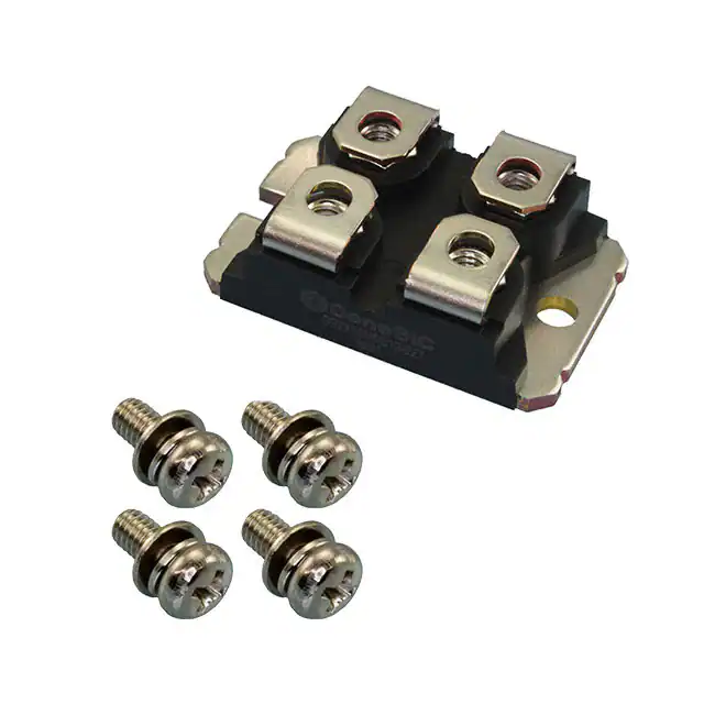
Package
Low VF for High Temperature Operation
Enhanced Surge and Avalanche Robustness
Superior Figure of Merit QC/IF
Low Thermal Resistance
Low Reverse Leakage Current
Temperature Independent Fast Switching
Positive Temperature Coefficient of VF
Low VF for High Temperature Operation
A
A
RoHS
SOT-227
Advantages
•
•
•
•
•
•
•
•
1700 V
100 A *
1076 nC *
K
K
REACH
Applications
Improved System Efficiency
High System Reliability
Optimal Price Performance
Reduced Cooling Requirements
Increased System Power Density
Zero Reverse Recovery Current
Easy to Parallel without Thermal Runaway
Improved System Efficiency
•
•
•
•
•
•
•
•
EV Fast Chargers
Solar Inverters
Wind Energy Converters
Train Auxiliary Power Supplies
High Frequency Rectifiers
Switched Mode Power Supplies
Motor Drives
Pulsed Power
Absolute Maximum Ratings (At TC = 25°C Unless Otherwise Stated)
Parameter
Repetitive Peak Reverse Voltage (Per Leg)
Continuous Forward Current (Per Leg / Per Device)
Non-Repetitive Peak Forward Surge Current, Half Sine
Wave (Per Leg)
Repetitive Peak Forward Surge Current, Half Sine Wave
(Per Leg)
Non-Repetitive Peak Forward Surge Current (Per Leg)
i2t Value (Per Leg)
Non-Repetitive Avalanche Energy (Per Leg)
Diode Ruggedness (Per Leg)
Power Dissipation (Per Leg / Per Device)
Operating and Storage Temperature
Symbol
VRRM
IF
IF,SM
IF,RM
IF,MAX
∫i2dt
EAS
dV/dt
PTOT
T j , T stg
Conditions
TC = 75°C, D = 1
TC = 100°C, D = 1
TC = 134°C, D = 1
TC = 25°C, tP = 10 ms
TC = 150°C, tP = 10 ms
TC = 25°C, tP = 10 ms
TC = 150°C, tP = 10 ms
T C = 25°C, t P = 10 µs
TC = 25°C, tP = 10 ms
L = 1.0 mH, IAS = 50 A
VR = 0 ~ 1360 V
TC = 25°C
Values
1700
84 / 168
71 / 142
50 / 100
500
400
300
210
2500
1250
1301
200
387 / 774
-55 to 175
Unit
V
Note
A
Fig. 4
A
A
A
A2s
mJ
V/ns
W
°C
Fig. 3
* Per Device
Rev 21/Mar
Latest Version at: www.genesicsemi.com/sic-schottky-mps/GB2X50MPS17-227/GB2X50MPS17-227.pdf
Page 1 of 7
�GB2X50MPS17-227
1700V 100A SiC Schottky MPS™ Diode
TM
Electrical Characteristics (Per Leg)
Parameter
Symbol
Diode Forward Voltage
VF
Reverse Current
IR
Total Capacitive Charge
QC
Switching Time
tS
Total Capacitance
C
Conditions
Min.
IF = 50 A, Tj = 25°C
IF = 50 A, Tj = 175°C
VR = 1700 V, Tj = 25°C
VR = 1700 V, Tj = 175°C
VR = 600 V
VR = 1200 V
IF ≤ IF,MAX
dIF/dt = 200 A/µs
VR = 600 V
VR = 1200 V
VR = 1 V, f = 1MHz
VR = 1200 V, f = 1MHz
Values
Typ.
1.5
2.1
2
42
368
538
Max.
1.8
10
Unit
Note
V
Fig. 1
µA
Fig. 2
nC
Fig. 7
< 10
ns
4701
259
pF
Fig. 6
Unit
Note
°C/W
Fig. 9
Thermal/Package Characteristics
Parameter
Symbol
Thermal Resistance, Junction - Case
(Per Leg)
Weight
Mounting Torque
Terminal Connection Torque
Isolation Voltage(RMS)
Creepage Distance on Surface
Striking Distance Through Air
Rev 21/Mar
Conditions
RthJC
WT
TM
TC
VISO
dCtt
dCtb
dStt
dStb
Min.
Values
Typ.
Max.
0.39
28.0
Screws to Heatsink
M4 Screws
t = 1s (50/60 Hz)
t = 60s (50/60 Hz)
Terminal to Terminal
Terminal to Backside
Terminal to Terminal
Terminal to Backside
1.5
1.3
3000
2500
10.5
8.5
3.2
6.8
Latest Version at: www.genesicsemi.com/sic-schottky-mps/GB2X50MPS17-227/GB2X50MPS17-227.pdf
g
Nm
Nm
V
mm
mm
Page 2 of 7
�GB2X50MPS17-227
1700V 100A SiC Schottky MPS™ Diode
Figure 1: Typical Forward Characteristics (Per Leg)
I F = f(VF,Tj); tP = 250 µs
Figure 3: Power Derating Curves (Per Leg)
PTOT = f(TC ); Tj = 175°C
Rev 21/Mar
TM
Figure 2: Typical Reverse Characteristics (Per Leg)
I R = f(VR,Tj)
Figure 4: Current Derating Curves (Typical VF) (Per Leg)
I F = f(TC ); D = tP/T; Tj ≤ 175°C; fSW > 10kHz
Latest Version at: www.genesicsemi.com/sic-schottky-mps/GB2X50MPS17-227/GB2X50MPS17-227.pdf
Page 3 of 7
�GB2X50MPS17-227
1700V 100A SiC Schottky MPS™ Diode
Figure 5: Current Derating Curves (Maximum VF) (Per
Leg)
I F = f(TC ); D = tP/T; Tj ≤ 175°C; fSW > 10kHz
Figure 7: Typical Capacitive Charge vs Reverse Voltage
Characteristics (Per Leg)
QC = f(VR); f = 1MHz
Rev 21/Mar
TM
Figure 6: Typical Junction Capacitance vs Reverse
Voltage Characteristics (Per Leg)
C = f(VR); f = 1MHz
Figure 8: Typical Capacitive Energy vs Reverse Voltage
Characteristics (Per Leg)
EC = f(VR); f = 1MHz
Latest Version at: www.genesicsemi.com/sic-schottky-mps/GB2X50MPS17-227/GB2X50MPS17-227.pdf
Page 4 of 7
�GB2X50MPS17-227
1700V 100A SiC Schottky MPS™ Diode
TM
Figure 9: Transient Thermal Impedance (Per Leg)
Zth,jc = f(tP,D); D = tP/T
Figure 10: Forward Curve Model (Per Leg)
Forward Curve Model Equation:
I F = (VF - VBI)/RDIFF (A)
Built-In Voltage (VBI):
VBI(Tj) = m × Tj + n (V)
m = -0.00128 (V/°C)
n = 0.99 (V)
Differential Resistance (RDIFF):
1/RDIFF
RDIFF(Tj) = a × Tj2 + b × Tj + c (Ω)
a = 2.03e-07 (Ω/°C2)
b = 7.11e-05 (Ω/°C)
c = 0.0093 (Ω)
VBI
Forward Power Loss Equation:
PLOSS = VBI(Tj) × I AVG + RDIFF(Tj) × I RMS2
I F = f(VF,Tj)
Rev 21/Mar
Latest Version at: www.genesicsemi.com/sic-schottky-mps/GB2X50MPS17-227/GB2X50MPS17-227.pdf
Page 5 of 7
�GB2X50MPS17-227
1700V 100A SiC Schottky MPS™ Diode
TM
Package Dimensions
SOT-227 Package Outline
0.472 (11.9)
0.480 (12.19)
0.372 (9.45)
0.378 (9.60)
1.240 (31.5)
1.255 (31.88)
0.310 (7.87)
0.322 (8.18)
0.108 (2.74)
0.124 (3.15)
Ø 0.163 (4.14)
0.169 (4.29)
R 3.97
0.163 (4.14)
0.169 (4.29)
0.990 (25.1)
1.000 (25.40)
0.495 (12.5)
0.506 (12.85)
0.172 (4.37)
0.186 (4.72)
0.191 (4.85)
0.234 (5.94)
0.080 (2.03)
0.084 (2.13)
M4
0.165 (4.19)
0.169 (4.29)
1.049 (26.6)
1.059 (26.90)
0.030 (0.76)
0.033 (0.84)
0.588 (14.9)
0.594 (15.09)
1.186 (30.1)
1.192 (30.28)
1.494 (37.9)
1.504 (38.20)
Package View
A
A
K
Isolated Base
K
NOTE
1. CONTROLLED DIMENSION IS INCH. DIMENSION IN BRACKET IS MILLIMETER.
2. DIMENSIONS DO NOT INCLUDE END FLASH, MOLD FLASH, MATERIAL PROTRUSIONS.
Rev 21/Mar
Latest Version at: www.genesicsemi.com/sic-schottky-mps/GB2X50MPS17-227/GB2X50MPS17-227.pdf
Page 6 of 7
�GB2X50MPS17-227
1700V 100A SiC Schottky MPS™ Diode
TM
Compliance
RoHS Compliance
The levels of RoHS restricted materials in this product are below the maximum concentration values (also referred to as the
threshold limits) permitted for such substances, or are used in an exempted application, in accordance with EU Directive
2011/65/EC (RoHS 2), as adopted by EU member states on January 2, 2013 and amended on March 31, 2015 by EU Directive
2015/863. RoHS Declarations for this product can be obtained from your GeneSiC representative.
REACH Compliance
REACH substances of high concern (SVHCs) information is available for this product. Since the European Chemical Agency
(ECHA) has published notice of their intent to frequently revise the SVHC listing for the foreseeable future, please contact a
GeneSiC representative to insure you get the most up-to-date REACH SVHC Declaration. REACH banned substance information
(REACH Article 67) is also available upon request.
Disclaimer
GeneSiC Semiconductor, Inc. reserves right to make changes to the product specifications and data in this document without
notice. GeneSiC disclaims all and any warranty and liability arising out of use or application of any product. No license, express or
implied to any intellectual property rights is granted by this document.
Unless otherwise expressly indicated, GeneSiC products are not designed, tested or authorized for use in life-saving, medical,
aircraft navigation, communication, air traffic control and weapons systems, nor in applications where their failure may result in
death, personal injury and/or property damage.
Related Links
• SPICE Models:
https://www.genesicsemi.com/sic-schottky-mps/GB2X50MPS17-227/GB2X50MPS17-227_SPICE.zip
• PLECS Models:
https://www.genesicsemi.com/sic-schottky-mps/GB2X50MPS17-227/GB2X50MPS17-227_PLECS.zip
• CAD Models:
https://www.genesicsemi.com/sic-schottky-mps/GB2X50MPS17-227/GB2X50MPS17-227_3D.zip
• Evaluation Boards: https://www.genesicsemi.com/technical-support
• Reliability:
https://www.genesicsemi.com/reliability
• Compliance:
https://www.genesicsemi.com/compliance
• Quality Manual: https://www.genesicsemi.com/quality
Revision History
• Rev 21/Mar: Updated with most recent data
• Supersedes: Rev 20/Apr, Rev 20/Aug
www.genesicsemi.com/sic-schottky-mps/
Rev 21/Mar
Copyright© 2021 GeneSiC Semiconductor Inc.
All Rights Reserved.
Published by GeneSiC Semiconductor, Inc.
43670 Trade Center Place Suite 155, Dulles, VA 20166; USA
Page 7 of 7
�