BLE 5, Thread, Zigbee Modules, BT840/F/E/X/XE
Ver 1.10 Aug. 2018
BluNor BT840F is a powerful, highly flexible, ultra low power Bluetooth Low Energy (BLE) using Nordic
nRF52840 SoC. With an ARM CortexTM M4F MCU, available 1MB flash, 256KB RAM, embedded 2.4GHz multiprotocol transceiver, and an integrated PCB trace antenna or u.FL connector for an external antenna. A power
amplifier is integrated in BT840X and BT840XE to increase Bluetooth range. It allows faster time to market with
reduced development cost.
Bluetooth ranges are measured in environments with Low Multiple Path Interference (LMPI) and antenna at 5
feet (1.52 meters), typical height of thermostat in the USA. Ranges for LMPI, correlating to actual link budget,
indicates the Bluetooth signal strength for penetrating walls in buildings.
Specifications:
nRF52840 QIAA, ARM Cortex M4F, 64 MHz
ARM® TrustZone® Cryptocell-310 co-processor
Complete RF solution with integrated antenna
BLE 5 data rate: 2Mbps, 1Mbps, 500kbps,
125kbps.
IEEE 802.15.4 Thread and Zigbee data rate: 250
Kbps
2.4 GHz proprietary data rate: 2 Mbps, 1 Mbps
Integrated DC-DC converter, inductors on
board.
Direct powered by Lithium batteries or USB
supply (up to 5.5V)
Serial Wire Debug (SWD)
Nordic SoftDevice Ready
Over-the-Air (OTA) firmware update
Flash/RAM: 1MB/256KB.
48 General purpose I/O pins
USB 2.0 full speed (12 Mbps) controller
QSPI 32 MHz interface
High speed 32 MHz SPI
Type 2 NFC-A tag with wake-on field, Touch-topair support
Programmable peripheral interconnect (PPI)
12 bit/200 Ksps ADC, 8 configurable channels
with programmable gain
64 level comparator
15 level comparator with wake-up from OFF
mode
Temperature sensor
4x4-channel pulse width modulator (PWM)
Audio peripherals: I2S, digital microphone
interface (PDM)
5 x 32 bit timers with counter mode
Up to 4x SPI masters/3x SPI slaves
Up to 2x I2C compatible 2-wire masters/slaves
2x UART (CTS/RTS)
Quadrature Demodulator (QDEC)
3x real time counters (RTC)
128-bit AES HW encryption
SoC Receiver Sensitivity: -96 dBm at 1Mbps
SoC TX power: programmable +8dBm to
-20dBm. Up to +6 dBi antenna gain.
Hybrid pins: 16 castellated and 45 LGA.
Integrated PCB trace antenna or u.FL connector
Operation voltage: 1.7V to 5.5V
Operation temperature: - 4 0 ° C t o + 8 5 ° C
QDID: 108621
Applications
Secure IoT
Beacons/Proximity
Connected appliances
Lighting products
Sensors
Home and building automation
Model Summaries
module
SoC
Size
BT Antenna
32.768 sleep crystal
BT range,1 Mbps, LMPI
BT range, 1Mbps, 1.52m
BT range, 125 Kbps, LMPI.
BT range, 125 kBps, 1.52m
FCC ID
IC ID
CE
Availability
BT840F
nRF52840-QIAA
15x20.8x1.9mm
PCB trace
External
1000 meters
390 meters
2300 meters
640 meters
X8WBT840
4100A-BT840
Certified
Production
BT840
nRF52840-QIAA
14x16x1.9mm
PCB trace
External
150 meters
120 meters
320 meters
210 meters
X8WBT840
4100A-BT840
Certified
Production
!1
BT840E
nRF52840-QIAA
14x16x1.9mm
u.FL
External
BT840X
nRF52840-QIAA
15x20.8x1.9mm
PCB trace + PA
Integrated
BT840XE
nRF52840-QIAA
15x20.8x1.9mm
PA + u.FL
Integrated
X8WBT840
4100A-BT840
Certified
Production
Pending
Pending
Pending
Pending
Sample
Sample 10/2018
�BLE 5, Thread, Zigbee Modules, BT840/F/E/X/XE
Ver 1.10 Aug. 2018
Table Of Contents
1. Introduction ........................................................................................................................................................3
BT840F Block Diagram ..................................................................................................................................... 3
BT840F ..............................................................................................................................................................3
BT840
4
BT840E..............................................................................................................................................................4
BT840X..............................................................................................................................................................4
BT840XE ........................................................................................................................................................... 4
2. Codes Development Using Nordic Tools ........................................................................................................... 5
Easy, fast and safe code development.............................................................................................................. 5
Over-The-Air DFU .............................................................................................................................................5
SoftDevices ....................................................................................................................................................... 5
Development Tools ............................................................................................................................................5
3. Product Descriptions .........................................................................................................................................6
Block Diagram of nRF52840 .............................................................................................................................6
ARM Trustzone CryptoCell 310 .........................................................................................................................7
Mechanical Drawings ........................................................................................................................................ 9
Pin Assignments of BT840 .............................................................................................................................. 12
Pin Function..................................................................................................................................................... 14
Mounting BT840F on the Host PCB ................................................................................................................ 16
Host Board Design for Low Cost or Long Range ............................................................................................ 17
Control Skyworks Power Amplifier................................................................................................................... 18
4. Bluetooth Range Measurements .....................................................................................................................21
5. AT Commands .................................................................................................................................................22
6. BT840F Evaluation Board ...............................................................................................................................22
Nordic Development Tools .............................................................................................................................. 23
Android OS Apps ............................................................................................................................................23
iOS Apps .........................................................................................................................................................23
BT840F V4 EvaluationBoard Schematics .......................................................................................................23
Suggestion for Battery Power Application .......................................................................................................24
7. Miscellaneous..................................................................................................................................................25
Soldering Temperature-Time Profile for Re-Flow Soldering ............................................................................ 25
Cautions, Design Notes, and Installation Notes .............................................................................................. 25
Packaging ........................................................................................................................................................ 28
FCC Label ....................................................................................................................................................... 28
Revision History .................................................................................................................................................. 29
8. Contact Us .......................................................................................................................................................30
!2
�BLE 5, Thread, Zigbee Modules, BT840/F/E/X/XE
Ver 1.10 Aug. 2018
1. Introduction
BluNor BT840F Series are powerful, highly flexible, ultra low power wireless modules using Nordic nRF52840
SoCs. With an ARM CortexTM M4F MCU, 1MB flash, 256KB RAM, embedded 2.4GHz multi-protocol
transceiver, and an integrated antenna, it allows faster time to market with reduced development cost.
The following is a block diagram of BT840F. Antenna circuit and main clock are integrated. All 48 GPIOs of
nRF52840 can be accessed from main board. For lower power consumption at idle state, a 32.768 kHz crystal
can be added on the host board. Connection to an external NFC (Near Field Communication) antenna is
provided.
BT840F Block Diagram
BlurNor BT840F is a sister module of BT832F. The physical size is the same. There are 21 additional LGA pins
for additional GPIOs provided by nRF52840.
There are 3 modules in the BT840F Series.
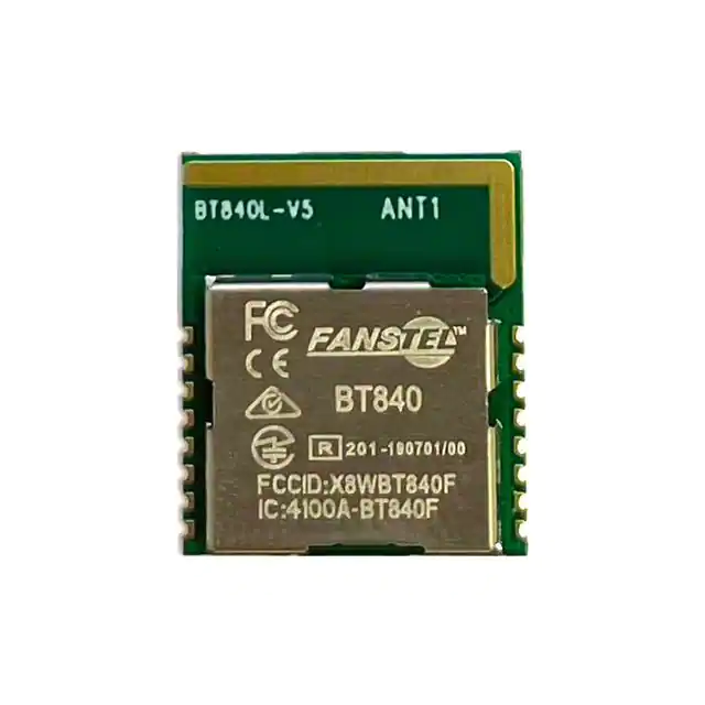
BT840F
•
Uses an nRF52840 QIAA with Cortex M4F MCU
•
1MB flash, 256 KB RAM
•
Supports NFC
•
Integrated PCB trace range antenna. Bluetooth range is 1000 meters at 1Mbps and
2300 meters at 125 Kbps measured in environments with low RF and multiple path
!3
�BLE 5, Thread, Zigbee Modules, BT840/F/E/X/XE
interferences.
•
Size: 15x20.8x1.9mm.
BT840
•
Uses an nRF52840 QIAA with Cortex M4F MCU
•
1MB flash, 256 KB RAM
•
Supports NFC
•
Integrated PCB trace range antenna.
•
Size: 14x16x1.9mm.
BT840E
•
Uses an nRF52840 QIAA with Cortex M4F MCU
•
1MB flash, 256 KB RAM
•
Supports NFC
•
An u.FL connector for external antenna. Certified with Fanstel ANT020 antenna..
•
Size: 14x16x1.9mm.
BT840X
•
Uses an nRF52840 QIAA with Cortex M4F MCU
•
1MB flash, 256 KB RAM
•
Supports NFC
•
Integrated SKY66112 power amplifier
•
Integrated 32.768 KHz sleep crystal
•
Integrated PCB trace antenna
•
Size: 15x28x1.9mm.
BT840XE
•
Uses an nRF52840 QIAA with Cortex M4F MCU
•
1MB flash, 256 KB RAM
•
Supports NFC
•
Integrated SKY66112 power amplifier.
•
Integrated 32.768 KHz sleep crystal.
•
An u.FL connector for external antenna.
•
Size: 15x28x1.9mm.
!4
Ver 1.10 Aug. 2018
�BLE 5, Thread, Zigbee Modules, BT840/F/E/X/XE
Ver 1.10 Aug. 2018
2. Codes Development Using Nordic Tools
Development tools by Nordic and other third party development tools recommended by Nordic should be
used .
Easy, fast and safe code development
Nordic development environment for nRF52840 offers a clean separation between application code
development and embedded protocol stacks. This means compile, link and run time dependencies with the
embedded stack and associated debugging challenges are removed. The Bluetooth low energy and ANT stack
is a pre-compiled binary, leaving application code to be compiled stand-alone. The embedded stack interface
uses an asynchronous and event driven model removing the need for RTOS frameworks.
Over-The-Air DFU
The nRF52840 is supported by an Over-The-Air Device Firmware Upgrade (OTA DFU) feature. This allows for
in the field updates of application software and SoftDevice.
SoftDevices
The Nordic protocol stacks are known as SoftDevices and complement the nRF52 Series SoCs. All nRF52
Series are programmable with software stacks from Nordic. This bring maximum flexibility to application
development and allows the latest stack version to be programmed into the SoC.
SoftDevices available from Nordic:
S140: Bluetooth low energy concurrent central/peripheral/observer/broadcaster stack.
Development Tools
Nordic Semiconductor provides a complete range of hardware and software development tools for the nRF52
Series devices. nRF52 DK board is recommended for firmware development.
Nordic software development tools can be downloaded from the following webpage.
http://infocenter.nordicsemi.com/index.jsp?topic=/com.nordic.infocenter.nrf52/dita/nrf52/development/
nrf52_dev_kit.html&cp=1_1
!5
�BLE 5, Thread, Zigbee Modules, BT840/F/E/X/XE
Ver 1.10 Aug. 2018
3. Product Descriptions
Brief description of nRF52840 SoC is provided. For full description of the SoC, please download from Nordic
Semiconductor website.
https://www.nordicsemi.com/eng/Products/Bluetooth-low-energy
Block Diagram of nRF52840
The following is a block diagram of Nordic nRF52840 Bluetooth Low Energy (BLE) SoC. Arrows with white
heads indicate signals that share physical pins with other signals.
!6
�BLE 5, Thread, Zigbee Modules, BT840/F/E/X/XE
Ver 1.10 Aug. 2018
The 32 bit ARM Cortex M4F MCU with hardware supports for DSP instructions and floating point operations,
code density and execution speed are higher than other Cortex M MCU. The Programmable Peripheral
Interconnect (PPI) system provides a 20-channel bus for direct and autonomous system peripheral
communication without CPU intervention. This brings predictable latency times for peripheral to peripheral
interaction and power saving benefits associated with leaving CPU idle. The device has 2 global power modes
ON/OFF, but all system blocks and peripherals have individual power management control which allows for an
automatic switching RUN/IDLE for system blocks based only on those required/not required to achieve
particular tasks.
The radio supports Bluetooth low energy and ANT. Output power is scalable from a maximum of +8dBm down
to -20 dBm in 4dB steps. Sensitivity is increased to -96 dBm to -89 dBm, depending on data rate. Sensitivity for
BLE is -96 dBm, and -92.5 dBm for ANT.
The NFC block supports NFC-A tags with proximity detection and Wake-on-field from low power mode. The
NFC enables Out-Of-Band (OOB) Bluetooth pairing of devices and thus greatly simplifying deployment.
ARM Trustzone CryptoCell 310
ARM® TrustZone® CryptoCell-310 co-processor is a security subsystem which provides Root of Trust (RoT) and
cryptographic services for a device. CryptoCell services are available to the application through a software library API, not
a hardware register interface.
!7
�BLE 5, Thread, Zigbee Modules, BT840/F/E/X/XE
Ver 1.10 Aug. 2018
The following cryptographic features are provided.
•
FIPS-140-2 certified True Random Number Generator (TRNG)
•
RSA asymmetric encryption
Up to 2048 bit key size
PKCS#1 v2.1/v1.5
Optional CRT support
•
Elliptic curve cryptography (ECC)
NIST FIPS 186-4 recommended curves using pseudo-random parameters, up to 521 bits:
➢ Prime field: P-192, P-224, P-256, P-384, P-521
SEC 2 recommended curves using pseudo-random parameters, up to 521 bits:
➢ Prime field: P-160, P-192, P-224, P-256, P-384, P-521
Koblitz curves using fixed parameters, up to 256 bits:
➢ Prime field: P-160, P-192, P-224, P-256
Edwards/Montgomery curves:
➢ Ed25519, Curve 25519
ECDH/ECDSA support
• Secure remote password protocol (SRP)
Up to 3072 bit operations
•
Hashing functions
SHA-1, SHA-2 up to 256 bit size
keyed-hash message authentication code (HMAC)
•
AES symmetric encryption
General purpose AES engine (encrypt/decrypt, sign/verify)
128 bit key size
Supported encryption modes: ECB, CBC, CMAC/CBC-MAC, CTR, CCM/CCM*.
•
ChaCha20/Poly1305 symmetric encryption
Supported keyed size: 128 and 256 bits
Authenticated encryption with associated data (AEAD) mode
!8
�BLE 5, Thread, Zigbee Modules, BT840/F/E/X/XE
Ver 1.10 Aug. 2018
Mechanical Drawings
The followings are mechanical drawings of BT840F and BT832F. The physical sizes of both are the same,
15x20.8x1.9mm. Except the 19 pins in solid black dots, BT840F and BT832F is hardware pin to pin compatible.
Firmware configuration is required to perform the same function.
Two types of pins are available to meet different application requirements.
• 16 castellated pins for application needing limited number of IOs. SMT equipment is not required for
soldering castellated pins.
• 45 LGA (Land Grid Array) pins to access all 48 GPIOs of nRF52840 when needed.
BT840F and BT832F Mechanical drawings, top view
!9
�BLE 5, Thread, Zigbee Modules, BT840/F/E/X/XE
BT840 and BT840E mechanical drawings, top view.
!10
Ver 1.10 Aug. 2018
�BLE 5, Thread, Zigbee Modules, BT840/F/E/X/XE
BT840X and BT840XE mechanical drawings
!11
Ver 1.10 Aug. 2018
�BLE 5, Thread, Zigbee Modules, BT840/F/E/X/XE
Ver 1.10 Aug. 2018
Pin Assignments of BT840
The followings are BT840 pin assignment. Pin functions are in a table in next section. Please refer to Nordic
nRF52840 Product Specifications for detailed descriptions and features supported.
https://www.nordicsemi.com/eng/Products/nRF52840
BT840F pins is a super set of that of BT832F. A PCB developed for BT832 Series can be used for BT840
Series and vice versa.
BT832F pin assignments.
!12
�BLE 5, Thread, Zigbee Modules, BT840/F/E/X/XE
BT840F pin assignments
!13
Ver 1.10 Aug. 2018
�BLE 5, Thread, Zigbee Modules, BT840/F/E/X/XE
Ver 1.10 Aug. 2018
Pin Function
BT840
52840
pin#
pin#
pin name
G1
P0.26/SDA
1
1
BT832
52832
pin#
pin#
pin name
Descriptions
38
P0.26
GPIO, configured as I2C SDA on EV-BT840
39
2
H2
P0.27/SCL
2
P0.27
GPIO, configured as I2C SCL on EV-BT840
3
D2
P0.00/XL1
3
2
P0.00/XL1
GPIO, connection for 32.768kHz crystal
4
F2
P0.01/XL2
4
3
P0.01/XL2
GPIO, connection for 32.768kHz crystal
5
A12
P0.02/AIN0
5
4
P0.02/AIN0
GPIO, Analog input
5
P0.03/AIN1
GPIO, Analog input
6
B13
P0.03/AIN1
6
7
L24
P0.09/NFC1
7
11
P0.09/NFC1
GPIO, NFC antenna connection
8
J24
P0.10/NFC2
8
12
P0.10/NFC2
GPIO, NFC antenna connection
13
9
B1
VDD
9
VDD
DC supply 1.7V to 3.6V
10
B7
GND
10
45
VSS
Ground
11
T2
P0.11
11
16
P0.13
GPIO
12
AD22
P1.00
12
21
P0.18
GPIO
23
13
AD8
P0.13
13
P0.20
GPIO
14
AC13
P0.18/RESET
14
24
P0.21/RESET
GPIO, configurable as RESET pin
15
AA24
SWDCLK
15
25
SWDCLK
Serial Wire Debug clock input
16
AC24
SWDIO
16
26
SWDIO
Serial Wire Debug I/O
Z0
B19
P1.11
GPIO
Z1
B17
P1.12
GPIO
Z2
A16
P1.13
GPIO
Z3
B15
P1.14
GPIO
Z4
A14
P1.15
GPIO
Z5
A20
P1.10
GPIO
Z6
R24
P1.06
GPIO
A0
GND
A0
45
VSS
Ground
A1
B11
P0.28/AIN4
A1
40
P0.28/AIN4
GPIO, Analog input
A2
A10
P0.29/AIN5
A2
41
P0.29/AIN5
GPIO, Analog input
A3
J1
P0.04/AIN2
A3
6
P0.04/AIN2
GPIO, Analog input
A4
K2
P0.05/AIN3
A4
7
P0.05/AIN3
GPIO, Analog input
A5
M2
P0.07
A5
9
P0.07
GPIO
A6
P2
P1.08
B0
GPIO
GND
B0
45
VSS
Ground
B1
AC21
P0.25
B1
37
P0.25
GPIO
B2
B9
P0.30/AIN6
B2
42
P0.30
GPIO
B3
A8
P0.31/AIN7
B3
43
P0.31
GPIO
B4
L1
P0.06
B4
8
P0.06
GPIO, NC for BT840X, BT840XE, PA control
B5
N1
P0.08
B5
10
P0.08
GPIO
B6
V23
P1.03
C0
GPIO
GND
C0
45
VSS
Ground
C1
AD20
P0.24
C1
29
P0.24
GPIO
C2
AD18
P0.22
C2
27
P0.22
GPIO
C3
AD12
P0.17
C3
20
P0.17
GPIO, NC for BT840X,BT840XE, PA control
!14
�BLE 5, Thread, Zigbee Modules, BT840/F/E/X/XE
C4
AD10
P0.15
C4
18
P0.15
GPIO
C5
W24
P1.02
C5
15
P0.12
GPIO
C6
U24
P1.04
GND
D0
45
VSS
Ground
D0
Ver 1.10 Aug. 2018
GPIO
D1
AC19
P0.23
D1
28
P0.23
GPIO
D2
AC15
P0.19
D2
22
P0.19
GPIO, NC for BT840 X,BT840XE, PA control
D3
AC11
P0.16
D3
19
P0.16
GPIO
D4
AC9
P0.14
D4
17
P0.14
GPIO
D5
Y23
P1.01
D5
14
P0.11
GPIO
D6
T23
P1.05
GPIO
E0
P23
P1.07
GPIO
E1
AD16
P0.20
GPIO
E2
AC17
P0.21
GPIO
E3
R1
P1.09
GPIO
E4
AD6
D+
USB D+
E5
AD4
D-
USB D-
E6
U1
P0.12
GPIO
F0
Ground pad
F1
Ground pad
F2
Ground pad
F3
Ground pad
F4
Y2
VDDH
High Voltage Power Supply
F5
AB2
DCCH
DC to DC converter output
F6
AD2
VBUS
5V DC power for USB 3.3V regulator
!15
�BLE 5, Thread, Zigbee Modules, BT840/F/E/X/XE
Ver 1.10 Aug. 2018
Mounting BT840F on the Host PCB
The following figure shows recommended mounting of BT840F module on the host PCB.
•
For the best Bluetooth range performance, the antenna area of module shall extend 9.8 mm outside the
edge of host PCB board, or 9.8 mm outside the edge of a ground plane.
•
The next choice is to place a module on a corner of host PCB, the antenna area shall extend 9.8 mm from
the edge of ground plane. Ground plane shall be at least 5 mm from the edge of the antenna area of
module.
•
We don’t recommend mounting BT840F module in the middle of a host PCB.
For the best Bluetooth range performance, keep all external metal at least 30mm from the antenna area.
!16
�BLE 5, Thread, Zigbee Modules, BT840/F/E/X/XE
Ver 1.10 Aug. 2018
Host Board Design for Low Cost or Long Range
On nRF52 series SoCs, Nordic offers various memory options and protocol supports. Fanstel offers various
antenna and power amplifier options. A host board can be designed to accommodate these nRF52 modules.
Our suggestions for host PCB design:
If your main goal is minimum PCB cost,
•
use a 2-sided PCB.
•
Use library component from EV BT832 Gerber files, can be downloaded from http://www.fanstel.com/
download-document/. It has 16 castellated pins plus 24 LGA pins. BT840F library component can be
used. However, signal routing can be difficult on a 2-sided PCB.
•
Be sure of no metal contact in the area of 21 additional BT840F pins.
•
BT840F can be mounted on a BT832 pad.
If you main goal is maximum wireless range,
•
use a 4 or more layers PCB.
•
Use library component from EV BT840F V4 or newer Gerber files, can be downloaded from http://
www.fanstel.com/download-document/. It has 16 castellated pins plus 45 LGA pins.
•
As much ground plane under BT840F, on top side of host PCB as possible. Use EV BT840F V4 Gerber
files as an example.
•
If your products may need wireless range of 1350 meters or more, allocate physical space for a
15x28x1.9mm module. This larger module size is required to accommodate Skyworks SKY66112 power
amplifier.
•
Don’t use P0.06 (BT840F pin B4), P0.17 (BT840F pin C3), and P0.19 (BT840F pin D2) on the host
board. These pins are used to control SKY66112 power amplifier in BT832X, BT832XE, BT840X and
BT840XE.
!17
�BLE 5, Thread, Zigbee Modules, BT840/F/E/X/XE
Ver 1.10 Aug. 2018
Control Skyworks Power Amplifier
BT840X uses SKYWORKS SKY66112-11 power amplifier. The connection diagram with control signal pins is
below.
5
4
3
2
1
D
D
VDD
UART
Filter
nRF52840
C
I2C
GPIO
P17
CTX
P19
CRX
P06
CPS
C
BT840 PCB ANT: 2.34dBi
BT840 SMA-J ANT: 6dBi
PA
SKY66112
ANT1
PCB ANT
1
B
B
X'TAL
RESET
32MHz
Frequency Band from 2402 MHz to 2480 MHz.
FANSTEL Corporation.
A
A
Title
BT840 Module
5
4
3
Size
A
Document Number
Date:
Friday, August 10, 2018
Rev
1.0
BLOCK
Sheet
2
1
of
1
1
A firmware configuration example to contol Skyworks SKY66112 power amplifier is below. This firmware file,
SKY66112_PAconfig.txt can be downloaded from http://www.fanstel.com/download-document/.
//PCA10040.h
//set the clock
#define NRF_CLOCK_LFCLKSRC
.rc_ctiv
{.source
= 0,
= NRF_CLOCK_LF_SRC_SYNTH,
\
.rc_temp_ctiv = 0,
\
.xtal_accuracy = NRF_CLOCK_LF_XTAL_ACCURACY_250_PPM}
!18
\
�BLE 5, Thread, Zigbee Modules, BT840/F/E/X/XE
//main.c
//config the PA/LNA
#ifdef APP_PA_LAN
#define APP_PA_PIN
17
#define APP_LNA_PIN
19
#define APP_CPS_PIN
6
#define APP_AMP_PPI_CH_ID_SET 0
#define APP_AMP_PPI_CH_ID_CLR 1
#define APP_AMP_GPIOTE_CH_ID
0
static void pa_lna_setup(void)
{
uint32_t err_code;
nrf_gpio_cfg_output(APP_CPS_PIN);
nrf_gpio_pin_clear(APP_CPS_PIN); //enable
nrf_gpio_cfg_output(APP_PA_PIN);
nrf_gpio_pin_clear(APP_PA_PIN); //
nrf_gpio_cfg_output(APP_LNA_PIN);
nrf_gpio_pin_clear(APP_LNA_PIN); //
static ble_opt_t pa_lna_opts = {
.common_opt = {
.pa_lna = {
.pa_cfg = {
.enable = 1,
!19
Ver 1.10 Aug. 2018
�BLE 5, Thread, Zigbee Modules, BT840/F/E/X/XE
.active_high = 1,
.gpio_pin = APP_PA_PIN
},
.lna_cfg = {
.enable = 1,
.active_high = 1,
.gpio_pin = APP_LNA_PIN
},
.ppi_ch_id_set = APP_AMP_PPI_CH_ID_SET,
.ppi_ch_id_clr = APP_AMP_PPI_CH_ID_CLR,
.gpiote_ch_id = APP_AMP_GPIOTE_CH_ID
}
}
};
NRF_GPIO->DIRSET |= (1