BMD-360 Data Sheet
Version 0.6 PRELIM
�BMD-360 Data Sheet
1
Version 0.6 PRELIM
Contents
1
2
3
4
5
6
7
8
Contents................................................................................................................................................ i
Introduction ......................................................................................................................................... 1
Features ............................................................................................................................................... 1
Applications ......................................................................................................................................... 1
Ordering Information .......................................................................................................................... 2
Block Diagram ..................................................................................................................................... 2
Quick Specifications ............................................................................................................................ 3
Pin Descriptions – BMD-360 ................................................................................................................ 4
8.1
Pin-out .......................................................................................................................................... 4
8.2
Pin Descriptions ........................................................................................................................... 4
9
Electrical Specifications ...................................................................................................................... 6
9.1
Absolute Maximum Ratings ......................................................................................................... 6
9.2
Operating Conditions ................................................................................................................... 6
9.3
General Purpose I/O ..................................................................................................................... 6
9.4
Peripheral pin assignments ......................................................................................................... 7
9.5
Module RESET............................................................................................................................... 7
9.6
Debug & Programming ................................................................................................................. 7
9.7
Clocks............................................................................................................................................ 7
9.7.1 32.768kHz Crystal (LFXO) (Preliminary) ................................................................................. 7
9.7.2 32.768kHz Clock Source Comparison .................................................................................... 8
10 Firmware .............................................................................................................................................. 9
10.1 Factory Image ............................................................................................................................... 9
10.2 SoftDevices ................................................................................................................................... 9
10.2.1 S112 ...................................................................................................................................... 9
10.3 MAC Address Info (Image Pending)............................................................................................ 10
11 Mechanical Data (Image Pending) .................................................................................................... 11
11.1 Dimensions ................................................................................................................................. 11
11.2 Recommended PCB Land Pads ................................................................................................. 11
11.3 Module Marking (Image Pending) .............................................................................................. 12
12 RF Design Notes ................................................................................................................................. 13
12.1 Recommended RF Layout & Ground Plane ............................................................................... 13
12.2 Mechanical Enclosure ................................................................................................................ 13
12.3 Antenna Patterns (Pending) ...................................................................................................... 14
12.3.1 X-Y Plane ............................................................................................................................. 14
12.3.2 Y-Z Plane ............................................................................................................................. 15
12.3.3 Z-X Plane ............................................................................................................................. 15
13 BMD-360-EVAL Development Kit ....................................................................................................... 16
14 Bluetooth Qualification ..................................................................................................................... 16
15 Regulatory Agency Approvals ........................................................................................................... 17
15.1 United States (FCC) (Pending) ................................................................................................... 17
15.1.1 Labeling & User Information Requirements ...................................................................... 17
15.1.2 RF Exposure ........................................................................................................................ 17
15.2 Canada (IC) (Pending) ................................................................................................................ 18
15.2.1 Labeling & User Information Requirements ...................................................................... 18
i
�BMD-360 Data Sheet
Version 0.6 PRELIM
15.2.2 RF Exposure ........................................................................................................................ 19
15.3 Europe (CE) (Pending) ................................................................................................................ 19
15.3.1 Labeling & User Information Requirements ...................................................................... 19
15.4 Australia / New Zealand (RCM) (Pending) ................................................................................. 19
15.5 Environmental ............................................................................................................................ 20
15.5.1 RoHS ................................................................................................................................... 20
15.5.2 REACH ................................................................................................................................. 20
15.5.3 California Proposition 65 (P65) .......................................................................................... 20
16 Solder Reflow Temperature-Time Profile......................................................................................... 20
16.1 Moisture Sensitivity Level .......................................................................................................... 20
17 Packaging and Labeling .................................................................................................................... 21
17.1 Carrier Tape Dimensions............................................................................................................ 21
17.2 Reel Packaging ........................................................................................................................... 21
17.3 Packaging Label (Image Pending) ............................................................................................. 22
18 Cautions ............................................................................................................................................. 23
19 Life Support and other High-Risk Use Warning ................................................................................ 23
20 Related Documents ........................................................................................................................... 24
21 Contact Information .......................................................................................................................... 24
22 List of Tables ...................................................................................................................................... 25
23 List of Figures ..................................................................................................................................... 25
24 Document History.............................................................................................................................. 26
ii
�BMD-360 Data Sheet
2
Version 0.6 PRELIM
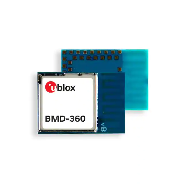
Introduction
The BMD-360 from Rigado is a powerful, highly flexible, ultra-low power Bluetooth 5.1 module based
on the nRF52811 SoC from Nordic Semiconductor. With an ARM® Cortex™ M4 CPU, embedded 2.4GHz
transceiver, and integrated antenna, it provides a complete RF solution with no additional RF design,
allowing faster time to market. Providing full use of the nRF52811’s capabilities and peripherals, the
BMD-360 can power demanding applications, while simplifying designs and reducing BOM costs. With
an internal DC-DC converter and intelligent power control, the BMD-360 provides class-leading power
efficiency, enabling ultra-low power sensitive applications. Regulatory pre-approvals reduce the
burden to enter the market. As a drop-in replacement for the BMD-300/301/330, the BMD-360
completes Rigado’s BMD-300 Series lineup with an optimized peripheral set that is attractive for a
wide range of cost-sensitive applications.
3
•
•
•
•
•
•
•
•
•
•
•
•
•
•
4
•
•
•
•
•
•
•
•
•
Features
Based on the Nordic nRF52811 SoC
Bluetooth 5.1 2M PHY, 1M PHY, Coded PHY
(long range), CSA #2, AoA, AoD
Complete RF solution with integrated DCDC converter
Nordic SoftDevice ready
Over-the-Air (OTA) firmware updates
No external components required
ARM® Cortex™-M4 32-bit processor
192kB embedded flash memory
24kB RAM
-40°C to +85°C Temperature Range
32 General Purpose I/O Pins
12-bit/200KSPS ADC
Serial Wire Debug (SWD)
SPI Master/Slave (8 Mbps)
•
•
•
•
•
•
•
•
2-wire Master/Slave (I2C compatible)
Footprint compatible with BMD-300,
BMD-301, BMD-330, BMD-340, and BMD341
UART (w/ CTS/RTS and DMA)
Low power comparator
Temperature sensor
20 channel CPU independent
Programmable Peripheral Interconnect
(PPI)
Quadrature Demodulator (QDEC)
128-bit AES HW encryption
3 x 32bit Real Timer Counters (RTC)
Dimensions: 14 x 9.8 x 1.9mm
USA (FCC): 2AA9B13 (Pending)
Canada (IC): 12208A-13 (Pending)
•
•
•
•
•
•
•
•
•
•
Internet of Things
Home Health Care
Advanced Remote Controls
Smart Energy Management
Low-Power Sensor Networks
Interactive Entertainment
Key Fobs
Environmental Monitoring
Hotel Automation
Office Automation
•
•
•
•
Applications
Beacons – iBeacon™, Eddystone,
AltBeacon, AoA, AoD
Low-Power Sensors
Fitness devices
Wearables
Climate Control
Lighting
Safety and Security
Home Appliances
Access Control
1
�BMD-360 Data Sheet
5
Version 0.6 PRELIM
Ordering Information
Part Number
Description
BMD-360-A-R
BMD-360-EVAL
BMD-360 module, Rev A, Tape & Reel, 1000-piece multiples
BMD-360 Evaluation Kit w/ SEGGER J-Link-OB debug probe
Table 1 – Ordering Information
6
Block Diagram
BMD-360 Bluetooth 5 Low Energy SoC Module
nRF52811-QFAx
24
kB RAM
SWD Debug &
Programming
Core LDO
DC/DC Buck
Regulator
DC-DC
Inductor
Accel Address
Resolver
ARM Cortex-M4
@ 64MHz
2.4GHz Radio
Multi-protocol
AES ECB
Balun
192kB
Flash
Matching
Network
AES CCM Mode
Encryption
Clock
Management
Real Time
Counter x2
Watchdog
Timer
Timer x3
Random Number
Gen
TWI
Master
SPI
Master
UART
TWI Slave
SPI Slave
4ch PWM
Bulk
Capacitors
Decoupling
Capacitors
Programmable
Peripheral
Interconnect
Temperature
Sensor
GPIO Task
Event Blocks
General
Purpose
Comparator
Quadrature
Decoder
8-ch 12-bit
ADC
PCB
Antenna
PDM
GPIO x32
(Analog x8)
32 MHz
Crystal
Figure 1 – Block Diagram
2
�BMD-360 Data Sheet
7
Version 0.6 PRELIM
Quick Specifications
Bluetooth
Version
Security
LE connections
Bluetooth 5 Low Energy, Peripheral (S112), 2M PHY, 1M PHY, Coded PHY, CSA #2, AoA/AoD
AES-128
Concurrent peripheral roles (S112)
Radio
Frequency
2.360GHz to 2.500GHz
Modulations
Transmit power
Receiver sensitivity
Antenna
GFSK at 1 Mbps, 2 Mbps data rates
+4 dBm maximum
-97 dBm (BLE 1M mode), -104dBm (Coded PHY mode)
Integrated (-1dBi peak)
Current Consumption
TX only @ +4 dBm, 0 dBm @ 3V, DCDC enabled
TX only @ +4 dBm, 0 dBm
RX only @ 1 Mbps @ 3V, DCDC enabled
RX only @ 1 Mbps
RX only @ 2 Mbps @ 3V, DCDC enabled
RX only @ 2 Mbps
CPU @ 64MHz from flash, from RAM
CPU @ 64MHz from flash, from RAM @ 3V, DCDC
System Off, On
Additional current for RAM retention
7.0 mA, 4.6 mA
15.4 mA, 10.1 mA
4.6 mA
10.0 mA
5.2 mA
11.2 mA
4.2 mA, 4.0 mA
2.2 mA, 2.1 mA
0.3 µA, 0.6 µA
30 nA / 4KB block
Dimensions
BMD-360
Length
Width
Height
14.0 mm ± 0.3mm
9.8 mm ± 0.3mm
1.9 mm ± 0.1mm
Hardware
Interfaces
Power supply
Temperature Range
SPI Master/Slave x 2
UART
Two-Wire Master/Slave (I2C)
1.7V to 3.6V
-40°C to +85°C
GPIO x 32
PWM
PDM
Certifications
USA (FCC) (Pending)
Canada (IC) (Pending)
Europe (CE) (Pending)
Australia / New Zealand (RCM)
(Pending)
Bluetooth (Pending)
FCC part 15 modular certification
FCC ID: 2AA9B13 (Pending)
Industry Canada RSS-210 modular certification
IC: 12208A-13 (Pending)
EN 60950-1: A2:2013 3.1 (a): Health and Safety of the User
EN 301 489-1 V2.1.1 & 3.1 (b): Electromagnetic Compatibility
EN 301 489-17 V3.1.1
EN 300 328 V2.1.1
3.2: Effective use of spectrum allocated
AS/NZS 4268:2017, Radio equipment and systems – Short range devices
BMD-360 BT5 RF-PHY Component (Tested) – DID: Pending; QDID: Pending
Export
BMD-360
ECCN: 5A992.C, Exception 740.17(b)(1)
HTS: 8473.30.1180
Nordic Semiconductor nRF52810
Additional details
nRF52810 Product Specification
Software Development Kit
Table 2 – Quick Specifications
3
�BMD-360 Data Sheet
8
8.1
Version 0.6 PRELIM
Pin Descriptions – BMD-360
Pin-out
The BMD-360 shares an identical pin-out with the BMD-300, BMD-301, and BMD-330. This pin-out is
also a subset of the BMD-340/341 footprint, allowing a single design to support any of these modules.
Figure 2 – BMD-360 Pin-out
8.2
Pin Descriptions
Pin
Name
Direction
Description
6
P0.25
In/Out
GPIO2
7
P0.26
In/Out
GPIO2
8
P0.27
In/Out
GPIO2
9
P0.28
In/Out
GPIO/AIN42
10
P0.29
In/Out
GPIO/AIN52
11
P0.30
In/Out
GPIO/AIN6
12
P0.31
In/Out
GPIO/AIN7
13
P0.00
In/Out
GPIO/XTAL1 (32.768kHz)
14
P0.01
In/Out
GPIO/XTAL2 (32.768kHz)
15
P0.02
In/Out
GPIO/AIN0
19
P0.03
In/Out
GPIO/AIN1
20
P0.04
In/Out
GPIO/AIN2
21
P0.05
In/Out
GPIO/AIN3
22
P0.06
In/Out
GPIO
23
P0.07
In/Out
GPIO
24
P0.08
In/Out
GPIO
25
P0.09
In/Out
GPIO
26
P0.10
In/Out
GPIO
27
P0.11
In/Out
GPIO
28
P0.12
In/Out
GPIO
31
P0.13
In/Out
GPIO
4
�BMD-360 Data Sheet
Version 0.6 PRELIM
Pin
Name
Direction
Description
32
P0.14
In/Out
GPIO
33
P0.15
In/Out
GPIO
34
P0.16
In/Out
GPIO
35
P0.17
In/Out
GPIO
36
P0.18
In/Out
GPIO
37
P0.19
In/Out
GPIO
38
P0.20
In/Out
GPIO
39
P0.21
In/Out
̅̅̅̅̅̅̅̅
GPIO/RESET
40
P0.22
In/Out
GPIO
41
P0.23
In/Out
GPIO
42
P0.24
In/Out
GPIO
43
SWCLK
In
SWD Clock
44
SWDIO
In/Out
SWD IO
17
VCC
Power
+1.7V to +3.6V1
1, 2, 3, 4, 5, 16,
18, 29, 30, 45,
46, 47
GND
Power
Electrical Ground
Note 1: An internal 4.7µF bulk capacitor is included on the module. However, it is good design practice to add
additional bulk capacitance as required for your application, i.e. those with heavy GPIO usage and/or current draw.
Note 2: These pins are in close proximity to the nRF52 radio power supply and antenna pins. Radio performance
parameters, such as sensitivity, may be affected by high frequency digital I/O (>10kHz) or with large sink/source
current on these pins. Nordic recommends using only low frequency, low-drive functions on these pins when possible.
Table 3 – Pin Descriptions
5
�BMD-360 Data Sheet
9
Version 0.6 PRELIM
Electrical Specifications
9.1
Absolute Maximum Ratings
Symbol
Parameter
Min.
Max.
Unit
VCC_MAX
Voltage on supply pin
-0.3
3.9
V
VIO_MAX
Voltage on GPIO pins (VCC > 3.6V)
-0.3
3.9
V
VIO_MAX
Voltage on GPIO pins (VCC ≤ 3.6V)
-0.3
VCC + 0.3V
V
TS
Storage Temperature Range
-40
125
°C
Table 4 – Absolute Maximum Ratings
9.2
Operating Conditions
Symbol
Parameter
Min.
Typ.
Max.
Unit
VCC
Operating supply voltage
1.7
3.0
3.6
V
TR_VCC
Supply rise time (0V to 1.7V)
-
-
60
ms
TA
Operating Ambient Temperature Range
-40
25
85
°C
Table 5 – Operating Conditions
9.3
General Purpose I/O
The general purpose I/O is organized as one port enabling access and control of the 32 available GPIO
pins through one port. Each GPIO can be accessed individually with the following user configurable
features:
•
•
•
•
•
•
•
Input/output direction
Output drive strength
Internal pull-up and pull-down resistors
Wake-up from high- or low-level triggers on all pins
Trigger interrupt on all pins
All pins can be used by the PPI task/event system; the maximum number of pins that can be
interfaced through the PPI at the same time is limited by the number of GPIOTE channels
All pins can be individually configured to carry serial interface or quadrature demodulator
signals
Symbol
Parameter
Min.
Typ.
Max.
Unit
VIH
Input High Voltage
0.7 x VCC
-
VCC
V
VIL
Input Low Voltage
VSS
-
0.3 x VCC
V
VOH
Output High Voltage
VCC − 0.4
-
VCC
V
VOL
Output Low Voltage
VSS
-
VSS + 0.4
V
RPU
Pull-up Resistance
11
13
16
kΩ
RPD
Pull-down Resistance
11
13
16
kΩ
Table 6 – GPIO
6
�BMD-360 Data Sheet
9.4
Version 0.6 PRELIM
Peripheral pin assignments
The various peripherals within the BMD-360 may be assigned to nearly any of the GPIO pins through
the application. There are some restrictions called out by the nRF52810 product specification. See
Note 2 in Table 6 above. Also note that certain peripherals are assigned to particular pins, such the
analog inputs.
9.5
Module RESET
GPIO pin P0.21 may be used for a hardware reset. In order to utilize P0.21 as a hardware reset, the
UICR registers PSELRESET[0] and PSELRESET[1] must be set alike, to the value of 0x7FFFFF15. When
P0.21 is programmed as ̅̅̅̅̅̅̅̅
RESET, the internal pull-up is automatically enabled. Rigado and Nordic
̅̅̅̅̅̅̅̅.
example applications and development kits program P0.21 as RESET
9.6
Debug & Programming
The BMD-360 Series supports the two pin Serial Wire Debug (SWD) interface and offers flexible and
powerful mechanism for non-intrusive debugging of program code. Breakpoints, single stepping, and
instruction trace capture of code execution flow are part of this support.
The BMD-360 also supports ETM and ITM trace. Trace data from the ETM and the ITM is sent to an
external debugger via a 4-bit wide parallel trace port. In addition to parallel trace, the TPIU supports
serial trace via the Serial Wire Output (SWO) trace protocol.
9.7
Clocks
The BMD-360 requires two clocks, a high frequency clock and a low frequency clock.
The high frequency clock is provided on-module by a high-accuracy 32MHz crystal as required by the
nRF52810 for radio operation.
The low frequency clock can be provided internally by an RC oscillator or synthesized from the fast
clock, or externally by a 32.768kHz crystal. An external crystal provides the lowest power consumption
and greatest accuracy. Using the internal RC oscillator with calibration provides acceptable
performance for BLE applications at a reduced cost and slight increase in power consumption. The
ANT protocol requires the use of an external crystal.
9.7.1
32.768kHz Crystal (LFXO) (Preliminary)
Symbol
Parameter
Typ.
Max.
Unit
FNOM_LFXO
Crystal frequency
32.768
-
kHz
FTOL_LFXO_BLE
Frequency tolerance, BLE applications1
-
±500
ppm
fTOL_LFXO_ANT
Frequency Tolerance, ANT applications
-
±50
ppm
CL_LFXO
Load Capacitance
-
12.5
pF
C0_LFXO
Shunt Capacitance
-
2
pF
RS_LFXO
Equivalent series resistance
-
100
kΩ
Cpin
Input Capacitance on XL1 & XL2 pads
4
-
pF
1
Note 1: fTOL_LFXO_BLE and fTOL_LFXO_ANT are the maximum allowed for BLE and ANT applications. Actual tolerance depends on
the crystal used.
Table 7 – 32.768kHz Crystal (LFXO)
7
�BMD-360 Data Sheet
9.7.2
Version 0.6 PRELIM
32.768kHz Clock Source Comparison
Symbol
Parameter
Min.
Typ.
Max. Unit
fTOL_LFXO_BLE
Frequency Tolerance, 32.768kHz Crystal Oscillator (BLE Stack)
1
-
-
±250
ppm
fTOL_LFXO_ANT
Frequency Tolerance, 32.768kHz Crystal Oscillator (ANT Stack)1
-
-
±50
ppm
f TOL_LFRC
Frequency Tolerance, 32.768kHz RC Oscillator
-
-
±2
%
fTOL_CAL_LFRC
Frequency tolerance, 32.768kHz RC after calibration
-
-
±500
ppm
fTOL_LFSYNT
Frequency Tolerance, 32.768kHz Synthesized Oscillator
-
-
±8
ppm
Note 1: fTOL_LFXO_BLE and fTOL_LFXO_ANT are the maximum allowed for BLE and ANT applications. Actual tolerance depends on
the crystal used.
Table 8 – 32.768kHz Clock Source Comparison
8
�BMD-360 Data Sheet
Version 0.6 PRELIM
10 Firmware
Rigado recommends that projects for the BMD-360 utilize Nordic Semiconductor's SDK, DFU, and
examples and the nRF52810 tools for any new development. This will allow access to the very latest
Bluetooth support from Nordic and provide an ongoing path as new features are released.
10.1 Factory Image
Due to the BMD-360’s reduced memory capacity, no factory firmware image is provided on the
module. This is indicated with a factory version code of “00” printed on the module label. Since there
is no bootloader on the module, firmware must be loaded on the module with the SWD interface.
10.2 SoftDevices
Nordic Semiconductor protocol stacks are known as SoftDevices. SoftDevices are pre-compiled, prelinked binary files. SoftDevices can be programmed in nRF52 series SoCs and are downloadable from
the Nordic website. The BMD-360 with the nRF52811 SoC supports the S112 (BLE Peripheral)
SoftDevices.
10.2.1 S112
The S112 SoftDevice is a Bluetooth low energy peripheral protocol stack solution. It supports up to
four peripheral connections with an additional broadcaster role running concurrently. The S112
SoftDevice integrates a Bluetooth low energy Controller and Host and provides a full and flexible API
for building Bluetooth low energy nRF52 System on Chip (SoC) solutions.
9
�BMD-360 Data Sheet
Version 0.6 PRELIM
10.3 MAC Address Info
The BMD-360 module comes preprogrammed with a unique MAC address from the factory. The MAC
address is also printed on a 2D barcode on the top of the module.
The 6-byte BLE Radio MAC address is stored in the nRF52810 UICR at NRF_UICR_BASE+0x80 LSB first.
Please read the MAC Address Provisioning application note to avoid erasing/overwriting the MAC
address during programming.
Figure 3 – BMD-360 MAC Address
UICR Register:
NRF_UICR + 0x80 (0x10001080): MAC_Addr [0] (0xZZ)
NRF_UICR + 0x81 (0x10001081): MAC_Addr [1] (0xYY)
NRF_UICR + 0x82 (0x10001082): MAC_Addr [2] (0xXX)
NRF_UICR + 0x83 (0x10001083): MAC_Addr [3] (0x93)
NRF_UICR + 0x84 (0x10001084): MAC_Addr [4] (0x54)
NRF_UICR + 0x85 (0x10001085): MAC_Addr [5] (0x94)
10
�BMD-360 Data Sheet
Version 0.6 PRELIM
11 Mechanical Data (Image Pending)
11.1 Dimensions
Figure 4 – Mechanical Drawing
11.2 Recommended PCB Land Pads
Figure 5 – Recommended PCB Land Pads
Note: The RF Keep-out area extends vertically to the board edge.
11
�BMD-360 Data Sheet
Version 0.6 PRELIM
11.3 Module Marking (Image Pending)
Figure 6 – Module Marking
12
�BMD-360 Data Sheet
Version 0.6 PRELIM
12 RF Design Notes
12.1 Recommended RF Layout & Ground Plane
For the BMD-360, the integrated antenna requires a suitable ground plane to radiate effectively.
The area under and extending out from the antenna portion of the module should be kept clear of
copper and other metal. The module should be placed at the edge of the PCB with the antenna edge
facing out. Reducing the ground plane from that shown in Figure 7 will reduce the effective radiated
power. For example, a 27mm x 29mm board (about the size of a coin cell) has approximately 3dB
lower output than the BMD-360 Evaluation Board.
These RF guidelines for the BMD-360 are the same as the BMD-300 module. Designs incorporating the
BMD-300 will have similar RF performance with the BMD-360 module.
Figure 7 – Recommended RF Layout & Ground Plane
12.2 Mechanical Enclosure
Care should be taken when designing and placing the BMD-360 into an enclosure. Metal should be
kept clear from the antenna area, both above and below. Any metal around the module can negatively
impact RF performance.
The module is designed and tuned for the antenna and RF components to be in free air. Any potting,
epoxy fill, plastic over-molding, or conformal coating can negatively impact RF performance and must
be evaluated by the customer.
13
�BMD-360 Data Sheet
Version 0.6 PRELIM
12.3 Antenna Patterns (Pending)
Antenna patterns are based on the BMD-300 Evaluation Kit with a ground plane size of 82mm x 56mm.
The BMD-300 module was replaced with a BMD-360 module. X-Y-Z orientation is shown in Figure 8:
Figure 8 – BMD-360-EVAL X-Y-Z Orientation
12.3.1 X-Y Plane
X
Y
Figure 9 – X-Y Plane Antenna Pattern
The outer-most ring is +5dB. Each division is -5dB
14
�BMD-360 Data Sheet
Version 0.6 PRELIM
12.3.2 Y-Z Plane
Y
Z
Figure 10 – Y-Z Plane Antenna Pattern
The outer-most ring is +5dB. Each division is -5dB
12.3.3 Z-X Plane
Z
X
Figure 11 – Z-X Plane Antenna Pattern
The outer-most ring is +5dB. Each division is -5dB
15
�BMD-360 Data Sheet
Version 0.6 PRELIM
13 BMD-360-EVAL Development Kit
The BMD-360-EVAL is a full featured evaluation board that provides a complete I/O pin out to headers,
on-board programming and debug, 32.768 kHz crystal, power & virtual COM port over USB, 4 user
LEDs, and 4 user buttons. The evaluation boards also provide the option to be powered from a CR2032
coin cell battery and have current sense resistors and headers to allow for convenient current
measurements. An Arduino Uno R3 style header is provided for easy prototyping of additional
functions. The evaluation boards also support programming off-board BMD-300 Series modules.
Figure 12 – BMD-360-EVAL
14 Bluetooth Qualification
•
•
•
•
•
The Bluetooth SIG maintains the Bluetooth Specification, and ensures that products are
properly tested and comply with the Bluetooth license agreements. Companies that list
products with the Bluetooth SIG are required to be members of the SIG and submit the listed
fees. Refer to this link for details: https://www.bluetooth.com/develop-withbluetooth/qualification-listing
The Rigado Bluetooth Low Energy modules based on Nordic Semiconductor SoCs are listed as
a “Tested Component”. This allows an end product based on a Rigado module to inherit the
component listings without the need to run through all of the tests again. The end product
will often inherit several different listings, known as Qualified Design IDs (QDID), and are
identified on a “Declaration of Compliance”. Refer to this Help Center article for creating a
Declaration of Compliance: https://rigado.zendesk.com/hc/en-us/articles/360002645694Bluetooth-SIG-Launch-Studio-Product-Declaration
The list of Qualified Products is found
here: https://launchstudio.bluetooth.com/Listings/Search
The BMD-360 primarily utilizes the S112 SoftDevice
A list of current QDIDs used by Rigado is maintained at the Rigado Help Center
16
�BMD-360 Data Sheet
Version 0.6 PRELIM
15 Regulatory Agency Approvals
15.1 United States (FCC) (Pending)
Rigado’s modules have received Federal Communications Commission (FCC) CFR47
Telecommunications, Part 15 Subpart C “Intentional Radiators” modular approval in accordance with
Part 15.212 Modular Transmitter approval. Modular approval allows the end user to integrate the
module into a finished product without obtaining subsequent and separate FCC approvals for
intentional radiation, provided no changes or modifications are made to the module circuitry.
Changes or modifications could void the user’s authority to operate the equipment. The end user
must comply with all of the instructions provided by the Grantee, which indicate installation and/or
operating conditions necessary for compliance.
The finished product is required to comply with all applicable FCC equipment authorizations
regulations, requirements and equipment functions not associated with the transmitter module
portion. For example, compliance must be demonstrated to regulations for other transmitter
components within the host product; to requirements for unintentional radiators (Part 15 Subpart B
“Unintentional Radiators”), such as digital devices, computer peripherals, radio receivers, etc.; and to
additional authorization requirements for the non-transmitter functions on the transmitter module
(i.e., Verification, or Declaration of Conformity) (e.g., transmitter modules may also contain digital
logic functions) as appropriate.
Caution! The OEM is still responsible for verifying end product compliance with FCC Part 15,
subpart B limits for unintentional radiators through an accredited test facility.
15.1.1 Labeling & User Information Requirements
The BMD-360 is assigned the FCC ID number: 2AA9B13 (Pending)
If the FCC ID is not visible when the module is installed inside another device, then the outside of the
finished product into which the module is installed must also display a label referring to the enclosed
module. This exterior label can use the following or similar wording:
Contains FCC ID: 2AA9B(Pending)
In addition to marking the product with the appropriate FCC ID, the end-product user manual may
also require specific information based on the digital device classification. Refer to the FCC Rules,
Title 47, Subchapter A, Part 15, Subpart B, Chapter §15.105 for specific wording of the notices.
15.1.2 RF Exposure
All transmitters regulated by FCC must comply with RF exposure requirements. KDB 447498 General
RF Exposure Guidance provides guidance in determining whether proposed or existing transmitting
facilities, operations or devices comply with limits for human exposure to Radio Frequency (RF) fields
adopted by the Federal Communications Commission (FCC).
This module is approved for installation into mobile and/or portable host platforms and must not be
co-located or operating in conjunction with any other antenna or transmitter except in accordance
with FCC multi-transmitter guidelines. End users must be provided with transmitter operating
conditions for satisfying RF Exposure compliance.
17
�BMD-360 Data Sheet
Version 0.6 PRELIM
15.2 Canada (IC) (Pending)
Rigado’s modules have been certified for use in Canada under Industry Canada (IC) Radio Standards
Specification (RSS) RSS-210 and RSSGen. Modular approval permits the installation of a module in a
host device without the need to recertify the device.
15.2.1 Labeling & User Information Requirements
The BMD-360 is assigned the IC ID number: 12208A-13 (Pending)
Labeling Requirements for the Host Device (from Section 3.2.1, RSS-Gen, Issue 3, December 2010): The
host device shall be properly labeled to identify the module within the host device. The Industry
Canada certification label of a module shall be clearly visible at all times when installed in the host
device, otherwise the host device must be labeled to display the Industry Canada certification number
of the module, preceded by the words “Contains transmitter module”, or the word “Contains”, or
similar wording expressing the same meaning, as follows:
Contains transmitter module IC: 12208A-(Pending)
User Manual Notice for License-Exempt Radio Apparatus (from Section 7.1.3 RSS-Gen, Issue 3,
December 2010): User manuals for license-exempt radio apparatus shall contain the following or
equivalent notice in a conspicuous location in the user manual or alternatively on the device or both:
This device complies with Industry Canada license exempt RSS standard(s). Operation is
subject to the following two conditions: (1) this device may not cause interference, and (2) this
device must accept any interference, including interference that may cause undesired
operation of the device.
Le présent appareil est conforme aux CNR d'Industrie Canada applicables aux appareils radio
exempts de licence. L'exploitation est autorisée aux deux conditions suivantes: (1) l'appareil
ne doit pas produire de brouillage, et (2) l'utilisateur de l'appareil doit accepter tout brouillage
radioélectrique subi, même si le brouillage est susceptible d'en compromettre le
fonctionnement.
Transmitter Antenna (from Section 7.1.2 RSS-Gen, Issue 3, December 2010): User manuals for
transmitters shall display the following notice in a conspicuous location:
Under Industry Canada regulations, this radio transmitter may only operate using an antenna
of a type and maximum (or lesser) gain approved for the transmitter by Industry Canada. To
reduce potential radio interference to other users, the antenna type and its gain should be so
chosen that the equivalent isotropically radiated power (e.i.r.p.) is not more than that
necessary for successful communication.
Conformément à la réglementation d'Industrie Canada, le présent émetteur radio peut
fonctionner avec une antenne d'un type et d'un gain maximal (ou inférieur) approuvé pour
l'émetteur par Industrie Canada. Dans le but de réduire les risques de brouillage
radioélectrique à l'intention des autres utilisateurs, il faut choisir le type d'antenne et son gain
de sorte que la puissance isotrope rayonnée équivalente (p.i.r.e.) ne dépasse pas l'intensité
nécessaire à l'établissement d'une communication satisfaisante.
18
�BMD-360 Data Sheet
Version 0.6 PRELIM
15.2.2 RF Exposure
All transmitters regulated by IC must comply with RF exposure requirements listed in RSS-102 - Radio
Frequency (RF) Exposure Compliance of Radiocommunication Apparatus (All Frequency Bands). This
module is approved for installation into mobile and/or portable host platforms and must not be colocated or operating in conjunction with any other antenna or transmitter except in accordance with
Industry Canada's multi-transmitter guidelines. End users must be provided with transmitter
operating conditions for satisfying RF Exposure compliance.
15.3 Europe (CE) (Pending)
The BMD-360 is a Radio Equipment Directive assessed radio module that is CE complaint and have
been manufactured and tested with the intention of being integrated into a final product.
The BME-300 has been tested to current Radio Equipment Directives
•
•
•
•
EN 60950-1: 2006 + A11: 2009 + A1: 2010 + A12: 2011 + A2: 2013
ETSI EN 300 328 V 2.1.1
ETSI EN 301 489-1 V2.1.1
ETSI EN 301 489-17 V3.1.1
The Radio Equipment Directive – Compliance Association (RED-CA) provides guidance on modular
devices at the RED-CA website: http://www.redca.eu/Pages/Documents%201.htm.
15.3.1 Labeling & User Information Requirements
The label on the final products which contain a Rigado module must follow CE marking requirements.
The “R&TTE Compliance Association Technical Guidance Note 01” provides guidance on final product
CE marking.
15.4 Australia / New Zealand (RCM) (Pending)
The BMD-360 has been tested to comply with the AS/NZS 4268:2017, Radio equipment and systems –
Short range devices – Limits and methods of measurement. The report may be downloaded from
www.rigado.com, and may be used as evidence in obtaining permission to use the Regulatory
Compliance Mark (RCM).
Information on registration as a Responsible Party, license and labeling requirements may be found at
the following websites:
Australia: http://www.acma.gov.au/theACMA/radiocommunications-short-range-devices-standard2004
New Zealand: http://www.rsm.govt.nz/compliance
Only Australian-based and New Zealand-based companies who are registered may be granted
permission to use the RCM. An Australian-based or New Zealand-based agent or importer may also
register as a Responsible Party to use the RCM on behalf of a company not in Australia or New
Zealand.
19
�BMD-360 Data Sheet
Version 0.6 PRELIM
15.5 Environmental
15.5.1 RoHS
Rigado’s modules are in compliance with Directive 2011/65/EU, 2015/863/EU of the European
Parliament and the Council on the restriction of the use of certain hazardous substances in electrical
and electronic equipment. The declaration may be found here: https://go.rigado.com/RoHS-Modules
15.5.2 REACH
Rigado’s modules listed below do not contain the 191 SVHC (Substance of Very High Concern), as
defined by Directive EC/1907/2006 Article according to REACH Annex XVII. The compliance statement
may be found here: https://go.rigado.com/REACH-Modules
15.5.3 California Proposition 65 (P65)
This product can expose you to Nickel (metallic), which is known to the State of California to cause
cancer. For more information go to www.P65Warnings.ca.gov. Warnings are not required where the
listed chemical is inaccessible to the average user of the end product.
16 Solder Reflow Temperature-Time Profile
Figure 13 – Reflow Profile for Lead Free Solder
16.1 Moisture Sensitivity Level
The BMD-360 is rated for MSL 3, 168-hour floor life after opening.
20
�BMD-360 Data Sheet
Version 0.6 PRELIM
17 Packaging and Labeling
17.1 Carrier Tape Dimensions
Figure 14 – Carrier Tape Dimensions
17.2 Reel Packaging
Modules are packaged on 330mm reels loaded with 1000 modules. Each reel is placed in an antistatic
bag with a desiccant pack and humidity card and placed in a 340x350x65mm box. An antistatic
warning and reel label are adhered to the outside of the bag.
Figure 15 – Reel Cartons
21
�BMD-360 Data Sheet
Version 0.6 PRELIM
17.3 Packaging Label
Figure 16 – Packaging Label
22
�BMD-360 Data Sheet
Version 0.6 PRELIM
18 Cautions
1) The guidelines of this document should be followed in order to assure proper performance of
the module.
2) This product is intended for use in office, business, and residential applications and not
designed for medical applications. See the life support policy below for use in medical
applications.
3) This module may short-circuit. If a short circuit can result in serious damage or injury, then
failsafe precautions should be used. This could be accomplished by redundant systems and
protection circuits.
4) Supply voltage to the module should not be higher than the specified inputs or reversed.
Additionally, it should not contain noise, spikes, or AC ripple voltage.
5) Avoid use with other high frequency circuits.
6) Use methods to eliminate static electricity when working with the module as it can damage
the components.
7) Contact with wires, the enclosure, or any other objects should be avoided.
8) Refer to the recommended land pattern when designing for this module.
9) If hand soldering is used, be sure to use the precautions outlined in this document.
10) This module should be kept away from heat, both during storage and after installation.
11) Do not drop or physically shock the module.
12) Do not damage the interface surfaces of the module.
13) The module should not be mechanically stressed at any time (storage, handling, installation).
14) Do not store or expose this module to:
• Humid or salty air conditions
• High concentrations of corrosive gasses.
• Long durations of direct sunlight.
• Temperatures lower than -40°C or higher than 125°C.
19 Life Support and other High-Risk Use Warning
This product is not designed nor intended for use in a life support device or system, nor for use in
other fault-intolerant, hazardous or other environments requiring fail-safe performance, such as any
application in which the failure or malfunction of the product could lead directly or indirectly to
death, bodily injury, or physical or property damage (collectively, “High-Risk Environments”). RIGADO
EXPRESSLY DISCLAIMS ANY EXPRESS OR IMPLIED WARRANTY OF FITNESS FOR USE IN HIGH-RISK
ENVIRONMENTS. The customer using this product in a High-Risk Environment agrees to indemnify and
defend Rigado from and against any claims and damages arising out of such use.
23
�BMD-360 Data Sheet
Version 0.6 PRELIM
20 Related Documents
Rigado Documents:
Visit the Rigado File Downloads page for BMD-360 documentation.
•
•
•
BMD-3xx-EVAL User Guide
BMD-300 Series Range Test
BMD-3xx-EVAL Reference Design
Nordic Documents:
Visit the Nordic InfoCenter for a comprehensive library of Nordic technical documentation.
•
•
nRF52811 Product Specification
nRF52811 S112 Soft Device Specification
21 Contact Information
Headquarters
Rigado Inc.
3950 Fairview Industrial Drive SE, Suite 100
Salem, Oregon 97302
Tel: +1 971 208 9870
Fax: +1 971 208 9869
Sales:
https://www.rigado.com/contact/
Support: https://rigado.zendesk.com/hc
24
�BMD-360 Data Sheet
Version 0.6 PRELIM
22 List of Tables
Table 1 – Ordering Information ................................................................................................................... 2
Table 2 – Quick Specifications ..................................................................................................................... 3
Table 3 – Pin Descriptions ............................................................................................................................ 5
Table 4 – Absolute Maximum Ratings.......................................................................................................... 6
Table 5 – Operating Conditions ................................................................................................................... 6
Table 6 – GPIO .............................................................................................................................................. 6
Table 7 – 32.768kHz Crystal (LFXO) ............................................................................................................. 7
Table 8 – 32.768kHz Clock Source Comparison .......................................................................................... 8
Table 9 – Document History....................................................................................................................... 26
23 List of Figures
Figure 1 – Block Diagram ............................................................................................................................. 2
Figure 2 – BMD-360 Pin-out .......................................................................................................................... 4
Figure 3 – BMD-360 MAC Address............................................................................................................... 10
Figure 4 – Mechanical Drawing .................................................................................................................. 11
Figure 5 – Recommended PCB Land Pads................................................................................................. 11
Figure 6 – Module Marking ......................................................................................................................... 12
Figure 7 – Recommended RF Layout & Ground Plane .............................................................................. 13
Figure 8 – BMD-360-EVAL X-Y-Z Orientation .............................................................................................. 14
Figure 9 – X-Y Plane Antenna Pattern ........................................................................................................ 14
Figure 10 – Y-Z Plane Antenna Pattern ...................................................................................................... 15
Figure 11 – Z-X Plane Antenna Pattern ...................................................................................................... 15
Figure 12 – BMD-360-EVAL ......................................................................................................................... 16
Figure 13 – Reflow Profile for Lead Free Solder ........................................................................................ 20
Figure 14 – Carrier Tape Dimensions ......................................................................................................... 21
Figure 15 – Reel Cartons............................................................................................................................. 21
Figure 16 – Packaging Label ...................................................................................................................... 22
25
�BMD-360 Data Sheet
Version 0.6 PRELIM
24 Document History
Revision
Date
Changes / Notes
0.5
2019-04-15
Preliminary release for engineering
0.6
2019-07-01
Corrected typos
Updated Nordic documentation link
Update images throughout
Table 9 – Document History
26
�