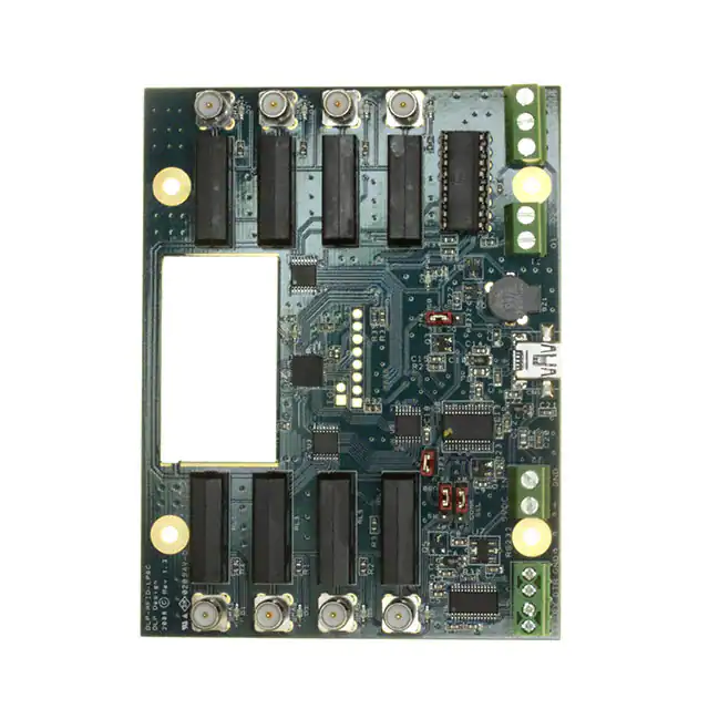
DLP-RFIDLP8C
LEAD-FREE
8-Channel Reader/Writer
FEATURES:
•
•
•
•
•
•
•
•
•
•
ISO15693, ISO14443A, ISO14443B Compatible
Can read the UID/SID of up to 15 Tags Simultaneously
13.56MHz Reader/Writer
8 Channels for External Antenna Connections
FCC/IC Modular Approvals in Place
USB Port Powered from Windows, CE or Linux PC
Both USB and RS232 Interfaces Provided
USB Interface; No Driver Development Required for Windows, CE or Linux PC
Operating Temperatures: 0°C to 70°C
Dimensions: (L x W x H) 4.36” x 3.32” x 0.6”
APPLICATIONS INCLUDE:
•
•
•
•
•
•
•
Real-Time Security
Personal Identification
Pharmaceutical Tracking
Inventory/Asset Management & Tracking
Library/Book Management & Tracking
Baggage Tagging
Sports Event Timing
1.0 INTRODUCTION
The DLP-RFID-LP8C is a low-cost, USB-powered module for reading from and writing to ISO15693,
ISO14443A and ISO14443B intelligent RFID transponder tags via up to eight external antennas. It has
the ability to both read and write tag user data in addition to reading the unique identifier (UID). All of the
DLP-RFID-LP8C’s electronics reside on a single, compact PCB; and all operational power is taken from
the host Windows/Windows CE/Linux PC via the USB interface. Up to eight external antennas can be
connected via reverse-polarity SMA connectors.
Rev. 1.7 (May 2018)
1
© DLP Design, Inc.
�2.0 HARDWARE SETUP
The four jumpers provided on the DLP-RFID-LP8C module are used to select between the USB and
Rs232 interfaces. For RS232 interface operation, move the three jumpers to the RS and RS232
positions and remove JP3. For USB operation, move the three jumpers to the USB position and add
jumper JP3.
If using the RS232 interface, connect the J3 wiring terminals to ±8V to ±12V serial signals typically found
in the DB9, RS232 port connectors on a host PC. An external, regulated 5 volt power source must also
be connected to J2.
If using USB, simply connect the DLP-RFID-LP8C to a host PC using the 5-pin mini-B USB connector
CN1 and a compatible USB cable. All power and data are provided via the USB cable.
3.0 APPLICATION DEVELOPMENT
The serial interface for the DLP-RFID-LP8C operates at 115,200 baud, no parity, 8 data bits and
1 stop bit.
A demonstration GUI is provided with the purchase of a DLP-RFID-LP8C module that demonstrates the
communications protocols. Using the Virtual COM Port USB drivers, the DLP-RFID-LP8C appears to the
host PC (Windows, Linux, Mac) as an RS232 port. The GUI presents the actual control packets sent,
and the reply data coming back from the DLP-RFID-LP8C as an aid to the software developer.
3.1 DEMONSTRATION GUI
The demonstration GUI is available as a free download from the DLP Design website. The URL for the
download page is printed on the outer packaging of the DLP-RFID-LP8C.
Rev. 1.7 (May 2018)
2
© DLP Design, Inc.
�3.2 LP8C SPECIFIC COMMANDS
To select one of the 8 external antennas on the DLP-RFID-LP8C you must send the correct command
packet (Ex: 010900030422F00000). To send this packet using the TI GUI, first make the connection to
the DLP-RFID-LP8C, and then click on the Test tab. Enter a command packet as shown below and click
on Send Raw. The LED associated with the antenna channel selected will light and successive tag reads
will use that channel.
LP8C Specific commands:
Commands to activate 1 of the 8 Antenna Channels:
1. 010900030422F00000
2. 010900030423F00000
3. 010900030424F00000
4. 010900030425F00000
5. 010900030426F00000
6. 010900030427F00000
7. 010900030428F00000
8. 010900030429F00000
Read Opto-isolated inputs:
010900030435F00000
Write opto-isolated output 1 high:
010900030430F00000
Write opto-isolated output 1 low:
010900030431F00000
Write opto-isolated output 2 high:
010900030432F00000
Write opto-isolated output 2 low:
010900030433F00000
Issue Pass beep
010900030477F00000
Issue Fail Beep
010900030479F00000
Rev. 1.7 (May 2018)
3
© DLP Design, Inc.
�3.3 LP8C OPERATING FIRMWARE
The source code for the firmware running in the DLP-RFID-LP8C reader (developed using Code
Composer Studio) is available for download upon purchase of the DLP-RFID-LP8C from the DLP Design
website.
4.0 MECHANICAL DIMENSIONS IN INCHES (MM)
2.08 typ
(53.0 typ)
0.45 typ
(11.4typ)
0.12 typ
(3.1 typ)
0.60 typ
(15.1 typ)
0.37 typ
(9.3 typ)
3.0 typ
(76.2typ)
1.55 typ
(39.4typ)
2.70 typ
(68.6typ)
3.84 typ
(97.6typ)
4.36 typ
(111 typ)
2.75 typ
(68.9 typ)
3.32 typ
(84typ)
Rev. 1.7 (May 2018)
2.85 typ
(72.3typ)
4
© DLP Design, Inc.
�5.0 REGULATORY AGENCY CONSIDERATIONS
5.1 AGENCY IDENTIFICATION NUMBERS
Compliance with the appropriate regulatory agencies is essential in the deployment of all intentional
radiators. DLP Design has obtained modular approval for this RF product such that an OEM need only
meet a few basic requirements in order to utilize their end product under this approval. Corresponding
agency identification numbers are listed below:
PART NUMBER
US/FCC
CAN/IC
DLP-RFID-LP8C
SX90LP8C
5675A-0LP8C
5.2 EXTERNAL ANTENNAS
The DLP-RFID1-LP8C is approved for use with external 50 Ohm loop/ferrite antennas that are resonant
at 13.56MHz. Connection is made via reverse-polarity SMA connectors.
Two different antennas are available from DLP Design: the DLP-FANT and the DLP-RFID-ANT.
DLP-FANT
DLP-RFID-ANT
The DLP-FANT ferrite-based antenna provides a compact footprint for space-constrained applications
and provides up to a 1.25-inch read range.
The DLP-FANT requires a coax cable with a reverse-polarity SMA connector at one end for connection
to the DLP-RFID-LP8C reader. This coax cable is available in a 3-foot length from DLP Design under
part number DLP-COAX1.
The DLP-RFID-ANT ships with an attached 15-foot coax cable with a reverse-polarity SMA connector
and provides up to 4 inches of read range with larger (credit card size) tags.
Rev. 1.7 (May 2018)
5
© DLP Design, Inc.
�5.3 FCC/IC REQUIREMENTS FOR MODULAR APPROVAL
Any changes or modifications to the DLP-RFID-LP8C’s printed circuit board could void the user’s
authority to operate the equipment. Operation of an unapproved antenna could void the user’s authority
to operate the equipment.
5.4 WARNINGS
Operation is subject to the following two conditions: (1) This device may not cause harmful interference;
and (2) this device must accept any interference received, including interference that may cause
undesirable operation.
To reduce potential radio interference with other users, the antenna type and its gain should be so
chosen that the equivalent isotropically-radiated power (e.i.r.p.) is not more than that permitted for
successful communication.
This device is intended for use under the following conditions:
1. The transmitter module may not be co-located with any other transmitter or antenna; and,
2. The module is approved using the FCC “unlicensed modular transmitter approval” method.
As long as these two conditions are met, further transmitter testing will not be required. However, the
OEM integrator is still responsible for testing their end product for any additional compliance measures
necessitated by the installation of this module (i.e. digital device emissions, PC peripheral requirements,
etc.).
Note: In the event that these conditions cannot be met (i.e. co-location with another transmitter), then
the FCC authorization is no longer valid, and the corresponding FCC ID may not be used on the final
product. Under these circumstances, the OEM integrator will be responsible for re-evaluating the end
product (including the transmitter) and obtaining a separate FCC authorization.
5.5 OEM PRODUCT LABELING
The final end product must be labeled in a visible area with the following text:
“Contains TX FCC ID: SX90LP8C”
5.6 RF EXPOSURE
In order to comply with FCC RF exposure-compliance requirements, the antenna used for this transmitter
must not be co-located or operating in conjunction with any other antenna or transmitter.
Rev. 1.7 (May 2018)
6
© DLP Design, Inc.
�5.7 ADDITIONAL INFORMATION FOR OEM INTEGRATORS
The end user should NOT be provided with any instructions on how to remove or install the DLP-RFIDLP8C. This device has been pre-certified to operate with the antenna models listed below, or any other
50 Ohm, magnetic loop antenna that resonates at 13.56MHz.
DLP Design Large Loop Antenna
DLP Design Small Loop Antenna
DLP Design Ferrite Antenna
6.0 DISCLAMER
Neither the whole nor any part of the information contained herein nor the product described in this
datasheet may be adapted or reproduced in any material or electronic form without the prior written
consent of the copyright holder.
This product and its documentation are supplied on an as-is basis, and no warranty as to their suitability
for any particular purpose is either made or implied. DLP Design will not accept any claim for damages
whatsoever arising as a result of use or failure of this product. Your statutory rights are not affected.
This product or any variant of it is not intended for use in any medical appliance, device or system in
which the failure of the product might reasonably be expected to result in personal injury.
This document provides preliminary information that may be subject to change without notice.
7.0 CONTACT INFORMATION
DLP Design, Inc.
1605 Roma Lane
Allen, TX 75013
Phone:
Fax:
Email:
Internet:
469-964-8027
415-901-4859
support@dlpdesign.com
http://www.dlpdesign.com
Rev. 1.7 (May 2018)
7
© DLP Design, Inc.
�D
5
RELAY SPST
RP-SMA1
RL1
901-144-8RFX
1
4
2
3
RELAY SPST
RL3
1
4
2
3
SWVCC
SWVCC
R1 R2 R3
360 360 360
D1 D3 D5 D7
LED LED LED LED
R4
360
SWVCC
16
15
14
13
12
11
10
4
COM
1B
2B
3B
4B
5B
6B
7B
9
1
2
3
4
5
6
7
U3
ULN2003A/TSSOP
1C
2C
3C
4C
5C
6C
7C
SWVCC
U4
ULN2003A/TSSOP
UCVCC
15
14
13
12
11
10
9
7
Y0
Y1
Y2
Y3
Y4
Y5
Y6
Y7
3
6
4
5
1
2
3
C18
0.1uF
A
B
C
G1
G2A
G2B
1
2
3
4
J3
RS232 Header
CN1
Mini-B USB Connector
1
2
3
4
5
U5
74HC238/TSSOP
ANT_SEL_A
ANT_SEL_B
ANT_SEL_C
UCVCC
C1
0.1uF
C2
0.1uF
J2
5VDC IN
2
FB1
240-1018-1
1
C10
10/10 Tant
C13
47pF
C11
.01
TX -->
RX
C12
47pF
1
2
5V IN
1
U6
C8
1uF/10V/0603
C5
0.1uF
4
3
IN
5
1
1
3.3V
D9
LED
Q4
MMBT3904
USBVCC
RESET
R28
360
FROMHOST
TX SELECT
C15
.1uF
47K
R23
SWVCC
C6
10/10 Tant
5V SELECT
.01uF/0603
C7
C9
.1uF
TOHOST
Q5
MMBT3904
RX Select
1
R21
30K
Q3
IRLML6402CT P
RX
USBVCC
COUT
OUT
U7
PQ1L303M2SP
CIN
C3
0.1uF
C4
0.1uF
R30
10K
23
22
13
14
12
1
5
3
11
2
9
10
6
RX
2
2
15
24
23
22
21
20
19
18
17
16
26
25
28
27
C21
0.1uF/0603
VCC
C1-
C1+
V+
FB2
240-1018-1
C2+
GND
C2VT1OUT
T2OUT
T3OUT
R1IN
R2IN
T4OUT
R3IN
T5OUT
INVALID
FORCEON
FORCEOFF
T1IN
T2IN
T3IN
R1OUT
R2OUT
T4IN
R3OUT
T5IN
R1OUTB
C19
10/10 Tant
C20
.01uF
1
2
3
4
5
6
7
8
9
10
11
12
13
14
MAX3238/SO
C14
.1uF
U8
USBDM
USBDP
VCC5 IN
FT232R
20
16
15
VCCIN/NC
RESET#
AVCC/NC
OSCI
OSCO
3V3OUT
1
1
2
3
4
5
6
7
9
8
19
24
27
28
17
FT232R
1
SWVCC
ANTENNA
R5 R6 R7
360 360 360
D2 D4 D6 D8
LED LED LED LED
R8
360
16
15
14
13
12
11
10
1B
2B
3B
4B
5B
6B
7B
COM
C22
.47uF
C16
.1uF
2
1
1
RELAY SPST
RL5
4
2
3
2
3
1
2
3
1
2
3
1C
2C
3C
4C
5C
6C
7C
SWVCC
3
GND
2
16
VCC
GND
8
CH1
RP-SMA3
901-144-8RFX
CH3
RP-SMA5
901-144-8RFX
CH5
4
2
3
RL7
RP-SMA7
RELAY SPST
901-144-8RFX
1
CH7
4
RELAY SPST
RL6
4
RELAY SPST
RL4
4
RELAY SPST
RP-SMA2
RL2
901-144-8RFX
1
CH2
RP-SMA4
901-144-8RFX
CH4
RP-SMA6
901-144-8RFX
CH6
RL8
RP-SMA8
RELAY SPST
901-144-8RFX
1
4
2
3
4
4
VCCIO
C
B
A
CH8
5
AGND
GND
GND
GND
TEST
25
7
18
21
26
GND
8
GND
8
D
C
B
A
�D
C
B
A
EXT_OUT1
EXT_OUT2
5
3VCC
R36
1.8K
R34
1.8K
5
16
R33
470
R32
470
1
15
14
11
10
2
3
9
13
12
6
7
4
5
8
ISO1
LTV846
C46
4
R31
10K
EXT_IN2
EXT_IN1
R35
10K
Y1
13.56MHz
3VCC
C33
2.2uF
SWVCC
22pF
4
3VCC
22pF
VDD_X
SYS_CLK
EN
VDD_A
VIN
VDD_RF
VDD_PA
TX_OUT
VSS_PA
VSS_RX
MOD
VDD_IO
VSS_D
VSS_A
ASK/OOK
IRQ
RX1_AM
BG
VSS
RX2_PM
IO7
IO6
IO5
IO4
IO3
IO2
IO1
IO0
DATA_CLK
EN2
XTAL_IN
XTAL_OUT
U1
TRF7970A
Matching
network &
filtration
C47
30
31
1
32
2
3
4
5
6
7
8
9
10
11
C34
0.01uF
3
J1
1
2
3
1
2
IN1
IN2
COM
OUT1
OUT2
J4
3VCC
3VCC
SLAVE_SELECT
SIMO
SOMI
DATA_CLK
SWVCC
ANTENNA
28
27
26
25
24
23
22
21
20
19
18
17
16
29
15
14
13
12
3
EXT_OUT1
EXT_OUT2
EXT_IN2
EXT_IN1
LED
SLAVE_SELECT
SIMO
SOMI
2
MMBT3904
Q1
R22
470
J5
PROGRAMMING HEADER
1
2
3
4
5
6
7
8
U2
MSP430F2370
P1.7/TA2
P2.0/ACLK/CA2
P2.1/TAINCLK/CA3
P2.2/CAOUT/TA0/CA4
P2.3/CA0/TA1
P2.4/CA1/TA2
P2.5/Rosc/CA5
P3.0/UCB0STE/UCA0CLK
P3.1/UCB0SIMO/UCB0SDA
P3.2/UCB0SOMI/UCB0SCL
DVCC
XIN/P2.6/CA6
XOUT/P2.7/CA7
P1.0/TACLK
P1.1/TA0
P1.2/TA1
P1.3/TA2
P1.4/SMCLK
P1.5/TA0
P1.6/TA1
SPKR
1
2
3
4
5
6
7
8
9
10
11
12
13
14
15
16
17
18
19
20
2
SWVCC
Q2
MMBT3904
37
36
35
34
BZ1
Buzzer
AVCC
D/AVSS
RST/NMI
P4.4/TB1
P4.3/TB0
P4.2/TB2
P4.1/TB1
P4.0/TB0
P3.7
P3.6
P3.5/UCA0RXD/UCA0SOMI
P3.4/UCA0TXD/UCA-SIMO
P3.3/UCB0CLK/UCA0STE
P4.7/TBCLK
P4.6/TBOUTH/ACLK
P4.5/TB2
TCK
TMS
TDI/TCLK
TDO/TDI
LED
40
39
38
33
32
31
30
29
28
27
26
25
24
23
22
21
R29
1
470
RESET
TG
C24
2.2uF
R19
100
Simplified
Schematic
D10
GR TAG LED
R20
47K
UCVCC
C25
0.01uF
47K
R37
1
2
Not used
Mode Sel
3VCC
DLP-RFID-LP8C
SPKR
ANT_SEL_C
ANT_SEL_B
ANT_SEL_A
FROMHOST
TOHOST
DATA_CLK
1
D
C
B
A
�