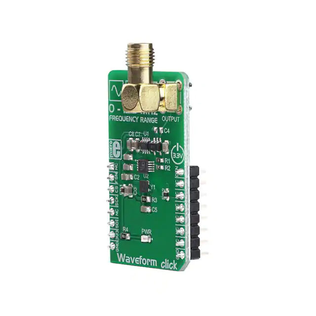
WAVEFORM CLICK
PID: MIKROE-3309
Weight: 27 g
Waveform Click is a precise sine/triangle/square waveform generator, capable of
reproducing frequencies up to 12MHz. It utilizes a Direct Digital Synthesis (DDS) IC
made by Analog Devices, a company famed for its specialization in DSP development
and engineering. The AD9833 waveform generator IC requires a very low count of
additional components: besides the external clock source, it requires almost no
components, allowing the Click board™ to be equipped with some additional circuits. A
digital potentiometer IC is used to attenuate the output signal, while the high-quality opamp is used as a buffer.
Waveform click is supported by a mikroSDK compliant library, which includes functions
that simplify software development. This Click board™ comes as a fully tested product,
ready to be used on a system equipped with the mikroBUS™ socket.
�HOW DOES IT WORK?
The main component of the Waveform click is the AD9833, a low-power, programmable
waveform generator, produced by Analog Devices. This company is well-established in
the market of high-quality Digital Signal Processing (DSP) solutions. The AD9833 IC is
based on the Direct Digital Synthesis (DDS), producing a waveform with the
programmable frequency and selectable wave shape at its output. The AD9833, along
with the AD5227, a digital potentiometer IC from the same company is controlled over
the SPI interface, allowing both the frequency and the amplitude to be changed very
quickly, without additional latency.
DDS is a method of producing an analog waveform, by exploiting the fact that the phase
of the signal is changed linearly. For simple periodic functions such as the sine function,
the phase changes linearly between 0 and 2π. This allows to build the Numerically
Controlled Oscillator (NCO) block, which outputs a numerical value that linearly
changes over time, in the range between 0 and 228 – 1 (since the AD9833 IC has a 28bit phase accumulator). The continuously changing output of the NCO block is used as
the index for the Lookup Table (LUT) which contains amplitudes of the output
waveform. The faster the NCO output changes, the higher the frequency of the output
signal, which is a basis for DDS. The main advantage over some other types of
synthesis (PLL for example), is its simplistic approach. The frequency can be changed
in very small steps (depending on the clock generator), while the maximum frequency
can easily reach GHz.
�Besides the NCO and the LUT, the AD9833 contains other blocks, necessary to
produce the waveform at the output. It also features a 10-bit DAC, which allows the
digital value to be translated into an analog voltage at the output. Since the ADC is only
10 bits wide, there is no need for the LUT to have too many elements. The resolution of
the ADC is the bottleneck, so just a slightly higher resolution is required for the LUT
data. This further reduces the complexity and costs. The AD9833 can completely avoid
using the LUT, producing a square wave (by using only the MSB of the DAC), with the
frequency that can be further multiplied by 2, and triangle wave (by redirecting the NCO
directly to DAC instead using it for sweeping through the LUT). The operating modes of
the AD9833 can be set up by using the config register over the SPI interface. For more
detailed information about the AD9833 IC, please refer to the datasheet of the AD9833.
However, the mikroSDK compatible library contains functions that simplify working with
the AD9833 IC.
The output of the AD9833 is routed to the AD5227 digital potentiometer, which is used
to set the amplitude of the output signal. This potentiometer is used to scale down the
amplitude in the range between 0V and 3.3V. It is controlled over the SPI interface. The
potentiometer is used since the AD9833 IC does not provide means to regulate the
amplitude of the signal at the output.
Waveform click uses the clock generator of 25MHz, which allows changing the
frequency in steps of 0.1Hz. High speed of the clock allows very high frequencies to be
produced, so this Click board™ can generate a very clean sine wave with the frequency
up to 5MHz, and square wave with the frequency up to 12MHz. The integrated clock
generator offers a STAND-BY pin, which is used to enable or disable the clock. If there
is a HIGH logic state on this pin, the clock generator will produce 25MHz clock signal.
This pin is pulled to VCC by a pull-up resistor, so by default the 25MHz clock generator
is enabled.
The output signal of the Click board™ is buffered by a low-noise op-amp, which
provides a constant impedance and limited protection to the whole circuit. It is available
over the SMA connector, allowing the shielded coaxial cable to be used.
�SPECIFICATIONS
Type
Measurements
Applications
It can be used in various applications, including test equipment, frequency
sweep/clock generators, line loss or attenuation testers, waveform
generators, in fluid flow measuring applications, and other similar applications
that require pulse, triangle, or sinusoidal waveform for their operation.
On-board
modules
AD9833, a low-power, programmable waveform generator; AD5227, a 64position digital potentiometer; ADA4891, a high speed, rail-to-rail operational
amplifier; all ICs from Analog Devices.
Key Features
Simple yet powerful waveform generator based on DSS, low power
consumption, 0 to 12MHz(5MHz sine) in steps of 0.1 Hz, 28-bit accumulator
resolution, integrated sinewave ROM LUT, high-quality SMA connector for
the signal protection, etc.
Interface
SPI
Input Voltage
3.3V
Click board
size
M (42.9 x 25.4 mm)
PINOUT DIAGRAM
This table shows how the pinout on Waveform Click corresponds to the pinout on the
mikroBUS™ socket (the latter shown in the two middle columns).
Notes
Chip Select for
AD9833
Pin
Pin
NC
1
AN
PWM
16
OEN
FSN
2
RST
INT
15
NC
Notes
Clock Generator Enable
�Chip Select for
AD5227
CS
3
CS
RX
14
NC
SCK
4
SCK
TX
13
NC
NC
5
MISO
SCL
12
NC
SPI Data IN
SDI
6
MOSI
SDA
11
NC
Power Supply
3V3
7
3.3V
5V
10
NC
Ground
GND
8
GND
GND
9
GND
SPI Clock
Ground
ONBOARD SETTINGS AND INDICATORS
Label
Name
Default
Description
LD1
PWR
-
Power LED indicator
CN1
OUTPUT
-
Output signal connector
SOFTWARE SUPPORT
We provide a library for the Waveform Click on our LibStock page, as well as a demo
application (example), developed using MikroElektronika compilers. The demo can run
on all the main MikroElektronika development boards.
Library Description
Library contains generic functions for controlling the waveform and frequency
output of the click board.
Key functions:
void waveform_sineOutput(uint32_t f) - Function for setting the sine wave output.
void waveform_triangleOutput(uint32_t f) - Function for setting the triangle wave output.
void waveform_squareOutput(uint32_t f) - Function for setting the square wave output.
�Examples description
The application is composed of the three sections :
System Initialization - Initialize the GPIO and communication structures.
Application Initialization - Initialization driver init, default configuration and sets first volume.
Application Initialization - Initialize the communication interface and configure the click board.
Application Task - Predefined characters are inputed from the serial port. Depending on the
character sent the signal frequency, waveform or amplitude will be changed.
void applicationTask()
{
char rxDat;
uint32_t freqTmp;
if(UART_Rdy_Ptr())
{
rxDat = UART_Rd_Ptr();
mikrobus_logWrite(&rxDat,_LOG_BYTE);
}
if(rxDat>0)
{
switch(rxDat)
{
case waveform_cmd[0]: {
waveform_digipotInc();
rxDat = 0;
break;
}
case waveform_cmd[1]: {
waveform_digipotDec();
rxDat = 0;
break;
}
case waveform_cmd[2]: {
freq += 1;
freqTmp = freq