BLE 5, Thread, Zigbee Modules, BT840/F/E/X/XE
Ver 1.11 May 2019
BluNor BT840F is a powerful, highly flexible, ultra low power Bluetooth Low Energy (BLE) using Nordic
nRF52840 SoC. With an ARM CortexTM M4F MCU, available 1MB flash, 256KB RAM, embedded 2.4GHz multiprotocol transceiver, and an integrated PCB trace antenna or u.FL connector for an external antenna. A power
amplifier is integrated in BT840X and BT840XE to increase Bluetooth range. It allows faster time to market with
reduced development cost.
Bluetooth ranges are measured in environments with Low Multiple Path Interference
(LMPI) and antenna at 5 feet (1.52 meters), typical height of thermostat in the USA.
Ranges for LMPI, correlating to actual link budget, indicates the Bluetooth signal
strength for penetrating walls in buildings.
Specifications:
nRF52840 QIAA, ARM Cortex M4F, 64 MHz
ARM® TrustZone® Cryptocell-310 co-processor
Complete RF solution with integrated antenna
BLE 5 data rate: 2Mbps, 1Mbps, 500kbps,
125kbps.
IEEE 802.15.4 Thread and Zigbee data rate: 250
Kbps
2.4 GHz proprietary data rate: 2 Mbps, 1 Mbps
Integrated DC-DC converter, inductors on
board.
Direct powered by Lithium batteries or USB
supply (up to 5.5V)
Serial Wire Debug (SWD)
Nordic SoftDevice Ready
Over-the-Air (OTA) firmware update
Flash/RAM: 1MB/256KB.
48 General purpose I/O pins
USB 2.0 full speed (12 Mbps) controller
QSPI 32 MHz interface
High speed 32 MHz SPI
Type 2 NFC-A tag with wake-on field, Touch-topair support
Programmable peripheral interconnect (PPI)
12 bit/200 Ksps ADC, 8 configurable channels
with programmable gain
64 level comparator
15 level comparator with wake-up from OFF
mode
Temperature sensor
4x4-channel pulse width modulator (PWM)
Audio peripherals: I2S, digital microphone
interface (PDM)
5 x 32 bit timers with counter mode
Up to 4x SPI masters/3x SPI slaves
Up to 2x I2C compatible 2-wire masters/slaves
2x UART (CTS/RTS)
Quadrature Demodulator (QDEC)
3x real time counters (RTC)
128-bit AES HW encryption
SoC Receiver Sensitivity: -96 dBm at 1Mbps
SoC TX power: programmable +8dBm to
-20dBm. Up to +6 dBi antenna gain.
Hybrid pins: 16 castellated and 45 LGA.
Integrated PCB trace antenna or u.FL connector
Operation voltage: 1.7V to 5.5V
Operation temperature: - 4 0 ° C t o + 8 5 ° C
QDID: 108621
Model Summaries
module
SoC
Size
BT Antenna
Peak TX
32.768 sleep crystal
BT range,1 Mbps, LMPI
BT range, 1Mbps, 1.52m
BT range, 125 Kbps, LMPI.
BT range, 125 kBps, 1.52m
FCC ID
IC ID
CE
Availability
BT840F
nRF52840-QIAA
15x20.8x1.9mm
PCB trace
BT840
nRF52840-QIAA
14x16x1.9mm
PCB trace
BT840E
nRF52840-QIAA
14x16x1.9mm
ANT002
External
1000 meters
390 meters
2300 meters
640 meters
X8WBT840
4100A-BT840
Certified
Production
External
150 meters
120 meters
320 meters
210 meters
X8WBT840
4100A-BT840
Certified
Production
External
!1
X8WBT840
4100A-BT840
Certified
Production
BT840X
nRF52840-QIAA
15x28.0x1.9mm
PCB trace + PA
+22.6 dBm
Integrated
1170 meters
900 meters
>4500 meters
1240 meters
X8WBT840X
4100A-BT840X
BT840XE
nRF52840-QIAA
15x28.0x1.9mm
PA+ANT000
+21.0 dBm
Integrated
1170 meters
1170 meters
>4500 meters
1920 meters
X8WBT840X
4100A-BT840X
Production
Production
�BLE 5, Thread, Zigbee Modules, BT840/F/E/X/XE
Ver 1.11 May 2019
Table Of Contents
1. Introduction ........................................................................................................................................................3
BT840F ..............................................................................................................................................................3
BT840 ................................................................................................................................................................4
BT840E..............................................................................................................................................................4
BT840X..............................................................................................................................................................4
BT840XE ........................................................................................................................................................... 4
2. Codes Development Using Nordic Tools ........................................................................................................... 5
Over-The-Air DFU .............................................................................................................................................5
SoftDevices ....................................................................................................................................................... 5
Development Tools ............................................................................................................................................5
3. Product Descriptions .........................................................................................................................................6
Block Diagram of nRF52840 .............................................................................................................................6
ARM Trustzone CryptoCell 310 .........................................................................................................................7
Mechanical Drawings ........................................................................................................................................ 9
Pin Assignments of BT840 .............................................................................................................................. 12
Pin Function..................................................................................................................................................... 14
Mounting BT840F on the Host PCB ................................................................................................................ 16
Host Board Design for Low Cost or Long Range ............................................................................................ 17
Control Skyworks Power Amplifier................................................................................................................... 18
4. Bluetooth Range Measurements .....................................................................................................................22
5. AT Commands .................................................................................................................................................24
6. BT840F Evaluation Board ...............................................................................................................................24
Nordic Development Tools............................................................................................................................... 25
Android OS Apps ............................................................................................................................................. 25
iOS Apps..........................................................................................................................................................25
BT840F V4 EvaluationBoard Schematics .......................................................................................................26
Suggestion for Battery Power Application .......................................................................................................27
7. Miscellaneous..................................................................................................................................................28
Soldering Temperature-Time Profile for Re-Flow Soldering ............................................................................ 28
Cautions, Design Notes, and Installation Notes .............................................................................................. 28
Packaging and Lot Number ............................................................................................................................. 32
FCC Label ....................................................................................................................................................... 32
Revision History .................................................................................................................................................. 33
Contact Us ..........................................................................................................................................................34
!2
�BLE 5, Thread, Zigbee Modules, BT840/F/E/X/XE
Ver 1.11 May 2019
1. Introduction
BluNor BT840F Series are powerful, highly flexible, ultra low power wireless modules using Nordic nRF52840
SoCs. With an ARM CortexTM M4F MCU, 1MB flash, 256KB RAM, embedded 2.4GHz multi-protocol
transceiver, and an integrated antenna, it allows faster time to market with reduced development cost.
The following is a block diagram of BT840F. Antenna circuit and main clock are integrated. All 48 GPIOs of
nRF52840 can be accessed from main board. For lower power consumption at idle state, a 32.768 kHz crystal
can be added on the host board. Connection to an external NFC (Near Field Communication) antenna is
provided.
BlurNor BT840F is a sister module of BT832F. The physical size is the same. There are 21 additional LGA pins
for additional GPIOs provided by nRF52840.
There are 3 modules in the BT840F Series.
BT840F
•
Uses an nRF52840 QIAA with Cortex M4F MCU
•
1MB flash, 256 KB RAM
•
Supports NFC
•
Integrated PCB trace range antenna. Bluetooth range is 1000 meters at 1Mbps and
2300 meters at 125 Kbps measured in environments with low RF and multiple path
interferences.
•
Size: 15x20.8x1.9mm.
!3
�BLE 5, Thread, Zigbee Modules, BT840/F/E/X/XE
BT840
•
Uses an nRF52840 QIAA with Cortex M4F MCU
•
1MB flash, 256 KB RAM
•
Supports NFC
•
Integrated PCB trace range antenna.
•
Size: 14x16x1.9mm.
BT840E
•
Uses an nRF52840 QIAA with Cortex M4F MCU
•
1MB flash, 256 KB RAM
•
Supports NFC
•
An u.FL connector for external antenna. Certified with Fanstel ANT020 antenna..
•
Size: 14x16x1.9mm.
BT840X
•
Uses an nRF52840 QIAA with Cortex M4F MCU
•
1MB flash, 256 KB RAM
•
Supports NFC
•
Integrated SKY66112 power amplifier
•
Integrated 32.768 KHz sleep crystal
•
Integrated PCB trace antenna
•
Size: 15x28x1.9mm.
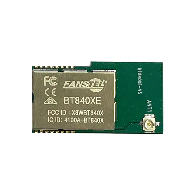
BT840XE
•
Uses an nRF52840 QIAA with Cortex M4F MCU
•
1MB flash, 256 KB RAM
•
Supports NFC
•
Integrated SKY66112 power amplifier.
•
Integrated 32.768 KHz sleep crystal.
•
An u.FL connector for external antenna. Certified with Fanstel ANT000 antenna.
•
Size: 15x28x1.9mm.
!4
Ver 1.11 May 2019
�BLE 5, Thread, Zigbee Modules, BT840/F/E/X/XE
Ver 1.11 May 2019
2. Codes Development Using Nordic Tools
Development tools by Nordic and other third party development tools recommended by Nordic should be used.
Nordic development environment for nRF52840 offers a clean separation between application code
development and embedded protocol stacks. This means compile, link and run time dependencies with the
embedded stack and associated debugging challenges are removed. The Bluetooth low energy and ANT stack
is a pre-compiled binary, leaving application code to be compiled stand-alone. The embedded stack interface
uses an asynchronous and event driven model removing the need for RTOS frameworks.
Over-The-Air DFU
The nRF52840 is supported by an Over-The-Air Device Firmware Upgrade (OTA DFU) feature. This allows for
in the field updates of application software and SoftDevice.
SoftDevices
The Nordic protocol stacks are known as SoftDevices and complement the nRF52 Series SoCs. All nRF52
Series are programmable with software stacks from Nordic. This bring maximum flexibility to application
development and allows the latest stack version to be programmed into the SoC.
SoftDevices available from Nordic:
S140: Bluetooth low energy concurrent central/peripheral/observer/broadcaster stack.
Development Tools
Nordic Semiconductor provides a complete range of hardware and software development tools for the nRF52
Series devices. nRF52 DK board is recommended for firmware development.
Nordic software development tools can be downloaded from the following webpage.
http://infocenter.nordicsemi.com/index.jsp?topic=/com.nordic.infocenter.nrf52/dita/nrf52/development/
nrf52_dev_kit.html&cp=1_1
!5
�BLE 5, Thread, Zigbee Modules, BT840/F/E/X/XE
Ver 1.11 May 2019
3. Product Descriptions
Brief description of nRF52840 SoC is provided. For full description of the SoC, please download from Nordic
Semiconductor website.
https://www.nordicsemi.com/eng/Products/Bluetooth-low-energy
Block Diagram of nRF52840
The following is a block diagram of Nordic nRF52840 Bluetooth Low Energy (BLE) SoC. Arrows with white
heads indicate signals that share physical pins with other signals.
!6
�BLE 5, Thread, Zigbee Modules, BT840/F/E/X/XE
Ver 1.11 May 2019
The 32 bit ARM Cortex M4F MCU with hardware supports for DSP instructions and floating point operations,
code density and execution speed are higher than other Cortex M MCU. The Programmable Peripheral
Interconnect (PPI) system provides a 20-channel bus for direct and autonomous system peripheral
communication without CPU intervention. This brings predictable latency times for peripheral to peripheral
interaction and power saving benefits associated with leaving CPU idle. The device has 2 global power modes
ON/OFF, but all system blocks and peripherals have individual power management control which allows for an
automatic switching RUN/IDLE for system blocks based only on those required/not required to achieve
particular tasks.
The radio supports Bluetooth low energy and ANT. Output power is scalable from a maximum of +8dBm down
to -20 dBm in 4dB steps. Sensitivity is increased to -96 dBm to -89 dBm, depending on data rate. Sensitivity for
BLE is -96 dBm, and -92.5 dBm for ANT.
The NFC block supports NFC-A tags with proximity detection and Wake-on-field from low power mode. The
NFC enables Out-Of-Band (OOB) Bluetooth pairing of devices and thus greatly simplifying deployment.
ARM Trustzone CryptoCell 310
ARM® TrustZone® CryptoCell-310 co-processor is a security subsystem which provides Root of Trust (RoT) and
cryptographic services for a device. CryptoCell services are available to the application through a software library API, not
a hardware register interface.
The following cryptographic features are provided.
!7
�BLE 5, Thread, Zigbee Modules, BT840/F/E/X/XE
•
FIPS-140-2 certified True Random Number Generator (TRNG)
•
RSA asymmetric encryption
Ver 1.11 May 2019
Up to 2048 bit key size
PKCS#1 v2.1/v1.5
Optional CRT support
•
Elliptic curve cryptography (ECC)
NIST FIPS 186-4 recommended curves using pseudo-random parameters, up to 521 bits:
➢ Prime field: P-192, P-224, P-256, P-384, P-521
SEC 2 recommended curves using pseudo-random parameters, up to 521 bits:
➢ Prime field: P-160, P-192, P-224, P-256, P-384, P-521
Koblitz curves using fixed parameters, up to 256 bits:
➢ Prime field: P-160, P-192, P-224, P-256
Edwards/Montgomery curves:
➢ Ed25519, Curve 25519
ECDH/ECDSA support
• Secure remote password protocol (SRP)
Up to 3072 bit operations
•
Hashing functions
SHA-1, SHA-2 up to 256 bit size
keyed-hash message authentication code (HMAC)
•
AES symmetric encryption
General purpose AES engine (encrypt/decrypt, sign/verify)
128 bit key size
Supported encryption modes: ECB, CBC, CMAC/CBC-MAC, CTR, CCM/CCM*.
•
ChaCha20/Poly1305 symmetric encryption
Supported keyed size: 128 and 256 bits
Authenticated encryption with associated data (AEAD) mode
!8
�BLE 5, Thread, Zigbee Modules, BT840/F/E/X/XE
Ver 1.11 May 2019
Mechanical Drawings
The followings are mechanical drawings of BT840F and BT832F. The physical sizes of both are the same,
15x20.8x1.9mm. Except the 19 pins in solid black dots, BT840F and BT832F is hardware pin to pin compatible.
Firmware configuration is required to perform the same function.
Two types of pins are available to meet different application requirements.
• 16 castellated pins for application needing limited number of IOs. SMT equipment is not required for
soldering castellated pins.
• 45 LGA (Land Grid Array) pins to access all 48 GPIOs of nRF52840 when needed.
BT840F and BT832F Mechanical drawings, top view
!9
�BLE 5, Thread, Zigbee Modules, BT840/F/E/X/XE
BT840 and BT840E mechanical drawings, top view.
!10
Ver 1.11 May 2019
�BLE 5, Thread, Zigbee Modules, BT840/F/E/X/XE
BT840X and BT840XE mechanical drawings
!11
Ver 1.11 May 2019
�BLE 5, Thread, Zigbee Modules, BT840/F/E/X/XE
Ver 1.11 May 2019
Pin Assignments of BT840
The followings are BT840 pin assignment. Pin functions are in a table in next section. Please refer to Nordic
nRF52840 Product Specifications for detailed descriptions and features supported.
https://www.nordicsemi.com/eng/Products/nRF52840
BT840F pins is a super set of that of BT832F. A PCB developed for BT832 Series can be used for BT840
Series and vice versa.
BT832F pin assignments.
!12
�BLE 5, Thread, Zigbee Modules, BT840/F/E/X/XE
BT840F pin assignments
!13
Ver 1.11 May 2019
�BLE 5, Thread, Zigbee Modules, BT840/F/E/X/XE
Ver 1.11 May 2019
Pin Function
BT840
52840
pin#
pin#
pin name
G1
P0.26/SDA
1
1
BT832
52832
pin#
pin#
pin name
Descriptions
38
P0.26
GPIO, configured as I2C SDA on EV-BT840
39
2
H2
P0.27/SCL
2
P0.27
GPIO, configured as I2C SCL on EV-BT840
3
D2
P0.00/XL1
3
2
P0.00/XL1
GPIO, connection for 32.768kHz crystal
4
F2
P0.01/XL2
4
3
P0.01/XL2
GPIO, connection for 32.768kHz crystal
5
A12
P0.02/AIN0
5
4
P0.02/AIN0
GPIO, Analog input
5
P0.03/AIN1
GPIO, Analog input
6
B13
P0.03/AIN1
6
7
L24
P0.09/NFC1
7
11
P0.09/NFC1
GPIO, NFC antenna connection
8
J24
P0.10/NFC2
8
12
P0.10/NFC2
GPIO, NFC antenna connection
13
9
B1
VDD
9
VDD
DC supply 1.7V to 3.6V
10
B7
GND
10
45
VSS
Ground
11
T2
P0.11
11
16
P0.13
GPIO
12
AD22
P1.00
12
21
P0.18
GPIO
23
13
AD8
P0.13
13
P0.20
GPIO
14
AC13
P0.18/RESET
14
24
P0.21/RESET
GPIO, configurable as RESET pin
15
AA24
SWDCLK
15
25
SWDCLK
Serial Wire Debug clock input
16
AC24
SWDIO
16
26
SWDIO
Serial Wire Debug I/O
Z0
B19
P1.11
GPIO
Z1
B17
P1.12
GPIO
Z2
A16
P1.13
GPIO
Z3
B15
P1.14
GPIO
Z4
A14
P1.15
GPIO
Z5
A20
P1.10
GPIO
Z6
R24
P1.06
GPIO
A0
GND
A0
45
VSS
Ground
A1
B11
P0.28/AIN4
A1
40
P0.28/AIN4
GPIO, Analog input
A2
A10
P0.29/AIN5
A2
41
P0.29/AIN5
GPIO, Analog input
A3
J1
P0.04/AIN2
A3
6
P0.04/AIN2
GPIO, Analog input
A4
K2
P0.05/AIN3
A4
7
P0.05/AIN3
GPIO, Analog input
A5
M2
P0.07
A5
9
P0.07
GPIO
A6
P2
P1.08
B0
GPIO
GND
B0
45
VSS
Ground
B1
AC21
P0.25
B1
37
P0.25
GPIO
B2
B9
P0.30/AIN6
B2
42
P0.30
GPIO
B3
A8
P0.31/AIN7
B3
43
P0.31
GPIO
B4
L1
P0.06
B4
8
P0.06
GPIO, NC for BT840X, BT840XE, PA control
B5
N1
P0.08
B5
10
P0.08
GPIO, NC for BT840X, BT840XE, PA control
B6
V23
P1.03
C0
GPIO
GND
C0
45
VSS
Ground
C1
AD20
P0.24
C1
29
P0.24
GPIO
C2
AD18
P0.22
C2
27
P0.22
GPIO
C3
AD12
P0.17
C3
20
P0.17
GPIO, NC for BT840X,BT840XE, PA control
!14
�BLE 5, Thread, Zigbee Modules, BT840/F/E/X/XE
C4
AD10
P0.15
C4
18
P0.15
GPIO
C5
W24
P1.02
C5
15
P0.12
GPIO
C6
U24
P1.04
GND
D0
45
VSS
Ground
D0
Ver 1.11 May 2019
GPIO
D1
AC19
P0.23
D1
28
P0.23
GPIO
D2
AC15
P0.19
D2
22
P0.19
GPIO, NC for BT840 X,BT840XE, PA control
D3
AC11
P0.16
D3
19
P0.16
GPIO
D4
AC9
P0.14
D4
17
P0.14
GPIO
D5
Y23
P1.01
D5
14
P0.11
GPIO
D6
T23
P1.05
GPIO
E0
P23
P1.07
GPIO
E1
AD16
P0.20
GPIO
E2
AC17
P0.21
GPIO
E3
R1
P1.09
GPIO
E4
AD6
D+
USB D+
E5
AD4
D-
USB D-
E6
U1
P0.12
GPIO
F0
Ground pad
F1
Ground pad
F2
Ground pad
F3
Ground pad
F4
Y2
VDDH
High Voltage Power Supply
F5
AB2
DCCH
DC to DC converter output
F6
AD2
VBUS
5V DC power for USB 3.3V regulator
!15
�BLE 5, Thread, Zigbee Modules, BT840/F/E/X/XE
Ver 1.11 May 2019
Mounting BT840F on the Host PCB
The following figure shows recommended mounting of BT840F module on the host PCB.
•
For the best Bluetooth range performance, the antenna area of module shall extend 9.8 mm outside the
edge of host PCB board, or 9.8 mm outside the edge of a ground plane.
•
The next choice is to place a module on a corner of host PCB, the antenna area shall extend 9.8 mm from
the edge of ground plane. Ground plane shall be at least 5 mm from the edge of the antenna area of
module.
•
We don’t recommend mounting BT840F module in the middle of a host PCB.
For the best Bluetooth range performance, keep all external metal at least 30mm from the antenna area.
!16
�BLE 5, Thread, Zigbee Modules, BT840/F/E/X/XE
Ver 1.11 May 2019
Host Board Design for Low Cost or Long Range
On nRF52 series SoCs, Nordic offers various memory options and protocol supports. Fanstel offers various
antenna and power amplifier options. A host board can be designed to accommodate these nRF52 modules.
Our suggestions for host PCB design:
If your main goal is minimum PCB cost,
•
use a 2-sided PCB.
•
Use library component from EV BT832 Gerber files, can be downloaded from http://www.fanstel.com/
download-document/. It has 16 castellated pins plus 24 LGA pins. BT840F library component can be
used. However, signal routing can be difficult on a 2-sided PCB.
•
Be sure of no metal contact in the area of 21 additional BT840F pins.
•
BT840F can be mounted on a BT832 pad.
If you main goal is maximum wireless range,
•
use a 4 or more layers PCB.
•
Use library component from EV BT840F V4 or newer Gerber files, can be downloaded from http://
www.fanstel.com/download-document/. It has 16 castellated pins plus 45 LGA pins.
•
As much ground plane under BT840F, on top side of host PCB as possible. Use EV BT840F V4 Gerber
files as an example.
•
If your products may need wireless range of 1350 meters or more, allocate physical space for a
15x28x1.9mm module. This larger module size is required to accommodate Skyworks SKY66112 power
amplifier.
•
Don’t use P0.06 (BT840F pin B4), P0.17 (BT840F pin C3), and P0.19 (BT840F pin D2) on the host
board. These pins are used to control SKY66112 power amplifier in BT832X, BT832XE, BT840X and
BT840XE.
!17
�BLE 5, Thread, Zigbee Modules, BT840/F/E/X/XE
Ver 1.11 May 2019
Control Skyworks Power Amplifier
BT840X uses SKYWORKS SKY66112-11 power amplifier. The connection diagram with control signal pins is
below.
A firmware example to control Skyworks SKY66112 power amplifier is below. This firmware file can be
downloaded from http://www.fanstel.com/download-document/.
You can set nRF52840 TX to up to + 8 dBm. The conditions for passing FCC and Industrial Canada
certification testings:
•
BT840X: Set nRF52840 TX to +2 dBm.
•
BT840XE: Set nRF52840 TX to +2 dB and use Fanstel antenna ANT000.
Header files
#ifndef PA_LNA_H__
#define PA_LNA_H__
#include "ble.h"
#include "app_error.h"
#include "nrf_drv_gpiote.h"
#include "nrf_drv_ppi.h"
void pa_lna_init(uint32_t gpio_pa_pin, uint32_t gpio_lna_pin);
#endif
!18
�BLE 5, Thread, Zigbee Modules, BT840/F/E/X/XE
Main program.
#include "pa_lna.h"
#define APP_PA_LAN
#ifdef APP_PA_LAN
#define APP_PA_PIN
#define APP_LNA_PIN
17
19
#define APP_CHL_PIN 8
#define APP_CPS_PIN
6
int main(void)
{
....
#ifdef APP_PA_LAN
nrf_gpio_cfg_output(APP_CPS_PIN);
nrf_gpio_cfg_output(APP_CHL_PIN);
nrf_gpio_pin_set(APP_CHL_PIN);
nrf_gpio_pin_clear(APP_CPS_PIN); //enable
pa_lna_init(APP_PA_PIN,APP_LNA_PIN);
#endif
....
}
SKY66112 control codes.
#include
#include
#include "pa_lna.h"
#include "ble.h"
#include "app_error.h"
#include "nrf_drv_gpiote.h"
#include "nrf_drv_ppi.h"
void pa_lna_init(uint32_t gpio_pa_pin, uint32_t gpio_lna_pin)
{
ble_opt_t opt;
uint32_t gpiote_ch = NULL;
!19
Ver 1.11 May 2019
�BLE 5, Thread, Zigbee Modules, BT840/F/E/X/XE
Ver 1.11 May 2019
ret_code_t err_code;
memset(&opt, 0, sizeof(ble_opt_t));
err_code = nrf_drv_gpiote_init();
if(err_code != NRF_ERROR_INVALID_STATE)
APP_ERROR_CHECK(err_code);
err_code = nrf_drv_ppi_init();
//if(err_code != MODULE_ALREADY_INITIALIZED)
APP_ERROR_CHECK(err_code);
nrf_ppi_channel_t ppi_set_ch;
nrf_ppi_channel_t ppi_clr_ch;
err_code = nrf_drv_ppi_channel_alloc(&ppi_set_ch);
APP_ERROR_CHECK(err_code);
err_code = nrf_drv_ppi_channel_alloc(&ppi_clr_ch);
APP_ERROR_CHECK(err_code);
nrf_drv_gpiote_out_config_t config = GPIOTE_CONFIG_OUT_TASK_TOGGLE(false);
if((gpio_pa_pin == NULL) && (gpio_lna_pin == NULL))
{
err_code = NRF_ERROR_INVALID_PARAM;
APP_ERROR_CHECK(err_code);
}
if(gpio_pa_pin != NULL)
{
if(gpiote_ch == NULL)
{
err_code = nrf_drv_gpiote_out_init(gpio_pa_pin, &config);
APP_ERROR_CHECK(err_code);
gpiote_ch = nrf_drv_gpiote_out_task_addr_get(gpio_pa_pin);
}
// PA config
opt.common_opt.pa_lna.pa_cfg.active_high = 1; // Set the pin to be active high
opt.common_opt.pa_lna.pa_cfg.enable
= 1; // Enable toggling
opt.common_opt.pa_lna.pa_cfg.gpio_pin = gpio_pa_pin; // The GPIO pin to toggle tx
}
if(gpio_lna_pin != NULL)
{
if(gpiote_ch == NULL)
{
err_code = nrf_drv_gpiote_out_init(gpio_lna_pin, &config);
APP_ERROR_CHECK(err_code);
!20
�BLE 5, Thread, Zigbee Modules, BT840/F/E/X/XE
Ver 1.11 May 2019
gpiote_ch = nrf_drv_gpiote_out_task_addr_get(gpio_lna_pin);
}
// LNA config
opt.common_opt.pa_lna.lna_cfg.active_high = 1; // Set the pin to be active high
opt.common_opt.pa_lna.lna_cfg.enable
= 1; // Enable toggling
opt.common_opt.pa_lna.lna_cfg.gpio_pin = gpio_lna_pin; // The GPIO pin to toggle rx
}
// Common PA/LNA config
opt.common_opt.pa_lna.gpiote_ch_id = (gpiote_ch - NRF_GPIOTE_BASE) >> 2; // GPIOTE channel used for
radio pin toggling
opt.common_opt.pa_lna.ppi_ch_id_clr = ppi_clr_ch; // PPI channel used for radio pin clearing
opt.common_opt.pa_lna.ppi_ch_id_set = ppi_set_ch; // PPI channel used for radio pin setting
err_code = sd_ble_opt_set(BLE_COMMON_OPT_PA_LNA, &opt);
APP_ERROR_CHECK(err_code);
}
!21
�BLE 5, Thread, Zigbee Modules, BT840/F/E/X/XE
Ver 1.11 May 2019
4. Bluetooth Range Measurements
Bluetooth range measurement reports and hex codes used in measurements can be downloaded from
Bluetooth Range Measurements section of this webpage.
http://www.fanstel.com/download-document/
Bluetooth ranges are measured between 2 modules on evaluation boards for various height of antenna. On the
first measurement, both antennas are pointing to sky and facing each other. The second antenna is rotated by
30 degrees clockwise after each measurement.
Bluetooth range is specified as the average of 12 measurements with the least significant digit truncated.
• 1.52 meters (60 inches) is typical height of thermostat in the USA.
• 0.55 meter (21.5 inches) is typical height of antenna if an IoT device is plugged into a wall AC outlet in the
USA. When USB840F USB dongle is plugged into a smart phone charger plugging into a wall AC outlet to
collect Bluetooth sensor data or to be used as a Bluetooth signal repeater.
• Low Multiple Path Interference (LMPI). For longer range measurement, antenna must be higher to have
LMPI. To have LMPI, 60% clearance is required. For example, if transmitter and receiver is 1000 meters
away, both antennas must be 3.33 meters above ground and away from any obstruction.
!22
�BLE 5, Thread, Zigbee Modules, BT840/F/E/X/XE
Ver 1.11 May 2019
The followings are Bluetooth range measurement results.
Antenna height
LMPI
1.52 meters
0.55 meter
BT840F Bluetooth range, 125Kbps
2300 meters
640 meters
210 meters
BT840F Bluetooth range, 1Mbps
1000 meters
390 meters
140 meters
BT840 Bluetooth range, 125 Kbps
320 meters
210 meters
BT840 Bluetooth range, 1Mbps
150 meters
120 meters
BT840X Bluetooth range, 125 Kbps
>4500 meters
1240 meters
BT840X Bluetooth range, 1Mbps
1170 meters
900 meters
BT840XE with ANT000 range, 125 Kbps
>4500 meters
1920 meters
BT840XE with ANT000 range, 1Mbps
1170 meters
1170 meters
• Bluetooth ranges of BT840X and BT840XE at 125 Kbps and LMPI, is verified to exceed 4500 meters,
maximum range of test site used in May 2019.
• Range of BT840XE with +21.0 dBm peak TX is longer than BT840X with +22.6 dBm peak TX. Antenna
ANT000 is almost omni-directional. The integrated antenna of BT840X is not. Range is shorter for some
angles. Result is the average of 12 measurements.
!23
�BLE 5, Thread, Zigbee Modules, BT840/F/E/X/XE
Ver 1.11 May 2019
5. AT Commands
AT command codes are used in production testing. They are not erased before shipping. If you develop your
own codes, please do chiperase and reprogram with your codes.
User manual and the newest AT Commands hex codes can be downloaded from AT Command Hex Codes,
Bluetooth 5 section of this web page.
http://www.fanstel.com/download-document/
AT commands can be used on UART interface and SPI interface. The preloaded codes use UART interface.
6. BT840F Evaluation Board
An evaluation board consists of the followings:
• Mini USB cable
• Evaluation board
• 10-conductor cable for connection to Nordic nRF52 DK (DK is not included)
!24
�BLE 5, Thread, Zigbee Modules, BT840/F/E/X/XE
Ver 1.11 May 2019
Nordic Development Tools
A Nordic nRF52 DK is recommended for programming this evaluation board. Nordic development tools can be
downloaded from:
https://www.nordicsemi.com/eng/Products/nRF52840
Many application examples can be downloaded from Nordic website.
Some firmware, Android OS, and iOS app codes can be downloaded from Bluetooth 5 Codes section of this
Fanstel webpage.
http://www.fanstel.com/download-document/
BT840 firmware can be used in all nRF52840 modules, e.g., BT840, BT840F, and BT840E.
Android OS Apps
The following Android OS apps are available for download from Google Play Store:
BlueNor nrf5x: to use with Bluetooth 5 stacks, AT commands, or Slave firmware. Master firmware does not
connect to a smartphone. Source codes can be downloaded from http://www.fanstel.com/download-document/
BlueNor Mesh: to use with BlueNor mesh firmware to send command to any node in a mesh. Node number is
displayed when acknowledgement is received. Source codes will be uploaded to Fanstel website when
supporting Bluetooth 5.
iOS Apps
The following iOS apps can be downloaded from Apple APP Store.
BlueNor Mesh: to use with BlueNor mesh firmware to send command to any node in a mesh. Node number is
displayed when acknowledgement is received.
BlueNor nrf5x firmware, apps, and source codes will be uploaded when ready.
!25
�BLE 5, Thread, Zigbee Modules, BT840/F/E/X/XE
Ver 1.11 May 2019
BT840F V4 EvaluationBoard Schematics
Evaluation board schematics and Gerber files can be downloaded from
http://www.fanstel.com/download-document/
4
P000(P00)
3
P001(P01)
4
P002(P02)
5
P003(P03)
6
P009(P09)
7
P010(P10)
8
P26/SDA
Z0
A0
B0
C0
D0
E0
Z1
A1
B1
C1
D1
E1
SWDIO
P27/SCL
SWCLK
P00/XL1
P01/XL2
Z2
A2
B2
C2
D2
E2
Z3
A3
B3
C3
D3
E3
P18/RESET
P13/LED
P02/AIN0
P100_SWO
P03/AIN1
P09/NFC1
Z4
A4
B4
C4
D4
E4
F4
Z5
A5
B5
C5
D5
E5
F5
Z6
A6
B6
C6
D6
E6
F6
P11/BUTTON
14
(P21) P018
13
(P20) P013
12
(P18) P100 SWO
11
(P13) P011
U1
GND
10uH
DCCH
Current measurement , SW6 all off
VDD
SW6
P102
P101
(P12)
(P11)
NC
CTS
RTS
RXD
TXD
DSR
DTR
GND
BAT-EN
1
2
3
4
5
6
7
2
4
120OHM
3
R7
3.01K
BAT-ADC
Y1
32.768KHz
GND
GND
14
13
12
11
10
9
8
CT1
10uF/10V
C8
1uF
GND
(P23)
1
2
P113
1
(P25)
1
P115
1
C9
0.1uF
GND
J21
GND
P101
P102
P011
P014
P015
P016
P017
P100
2
(ARDUINO)
J13
J9
2
1
3
5
2
RESET
5VIN
J4
2
4
6
P010
P009
P008
P007
P006
P005
P018
P001
P000
DETECT
J15
1
2ICSP
VDD
J16
MICRO
R10
47R 1/2W
C3
47uF / 10V
3
2
1
S1
1
R13
100K
GND
VDD
C
1
2
3
4
5
6
7
8
9
(P10)
(P09)
(P08)
(P07)
(P06)
(P05)
(P21)
(P01)
(P00)
Q4
A42
L1
2
1
5VIN
120OHM
1
1
2
R12
100K
3
4
U2
TCR3DF33
VI
VO
NC
3
EN
GND
3V3
5
4
C5
10uF / 10V
2
5
GND
GND
C
GND
GND
SW7 pin2-3 off ,
1
2
VDD
SW7
4
3
1
3
5
7
9
VDD
R15
1R 1%
GND
OFF ON
J19
Current meter
1
3
5
7
9
2
4
6
8
10
2
4
6
8
10
SWDIO
SWCLK
SWO
RESET
1
2
3
4
VDD
DEBUG - IN
JS2
1
2
3
4
CON4
GND
A
FANSTEL Corporation.
1
2
GND
JS1
VDD
J19 connect Current meter
3V3
3V3
R14
1K
GND
GND
SW7 pin2-3 on , J20 connect Oscilloscope
3V
GND
A
LED5
Current measurement , SW7 pin1-4 off
B
C4
10nF
C6
10uF / 10V
GND
3V
1
2
3
4
5
6
7
8
(D0 RX)
(D1 TX)
(D2)
(D3)
(D4)
(D5)
(D6)
(D7)
(P11)
(P12)
(P13)
(P14)
(P15)
(P16)
(P17)
(P18)
J11
R9
1M
1
2
4
J6
1
2
3
4
5
6
(A0)
(A1)
(A2)
(A3)
(A4)
(A5)
2
GND
R11
10K
J18
External supply
1
2
J8
P003(P03)
P004(P04)
P028(P28)
P029(P29)
P030(P30)
P031(P31)
D
GND
GND
5
2
Q3
A92
GND
GND
GND
J7
1
2
3
4
5
6
7
8
9
10
J5
AT_COM
BAT-ADC
BAT-EN
GND
5V
1
RST
GND
1
R8
1K 1%
C2
12pF nop
D-
2
P103
P104
P105
P106
P107
P012
P020
P021
J10
R6
10K
A
C7
0.1uF
1
P114
J2
P019(P19) (D8)
P013(P20) (D9)
P022(P22) (D10 SS)
P023(P23) (D11 MOSI)
P024(P24) (D12 MISO)
P025(P25) (D13 SCK)
GND
P002(P02) (AREF)
P026(P26) (SDA)
P027(P27) (SCL)
J12
D+
NC
NC
SUSPEND
SUSPEND
NC
RST
VBUS
1
5
+
R16
10K / 1%
(P24)
Q2
2N7002/SOT
ID
DCD
RI
GND
D+
DVDD
REGIN
1
3
5
7
9
11
13
15
G
NC
NC
NC
NC
NC
NC
NC
2
4
6
8
10
12
14
16
GND
1
2
3
4
5
6
7
8
VDD
VDD
RESET
VDD
5V
GND
GND
P018(P21)
5VIN
5VIN
L2
VDD
R4
1K
R5
10K
GND
Q1
TP0610T
S3
S1
22
23
24
25
26
27
28
29
U3
CP2102
21
20
19
18
17
16
15
J14
3V Battery
S4
S2
GND
P003(P03) AT_COM
J17
mini USB (PC)
P108
P109
P110
P111
P112
P113
P114
P115
2
J1
S2
S4
1
2
OFF ON
1
VDD
R3
1K
A
RESET1
VDD
R2
1K
A
2
4
3
UART_TX
UART_RX
LED3
(P20) C
A
LED4
OFF ON
C11
4.7uF
B
P013
GND
1
2
SW5 off , GPIO
SW5 on , 32K768Hz
OFF ON
GND
GND
3V3
C1
12pF nop
4
3
LED2
J14 input , J16 off
832X
2
VDDH
L3
1
2
1
2
P001(P01)
P000(P00)
2
(P19) C
C10
DNP
SW5
GND
SW4
(P18) C
P019
1
VDD
R1
1K
J3
VDD
1
SW8
4
3
VDD
2
P100
GND
GND
P023 (P23)
P019 (P19)
P016 (P16)
P014 (P14)
P101 (P11)
P105
P107
P020
P021
P109
D+
DP012
VDDH
DCCH
VBUS
P024 (P24)
P022 (P22)
P017 (P17)
P015 (P15)
P102 (P12)
P104
P025 (P25)
P030 (P30)
P031 (P31)
P006 (P06)
P008 (P08)
P103
P028 (P28)
P029 (P29)
P004 (P04)
P005 (P05)
P007 (P07)
P108
L3 Open , SW8 ON
(P16) 1
SWCLK
Z0
Z1
Z2
Z3
Z4
Z5
Z6
A0
A1
A2
A3
A4
A5
A6
B0
B1
B2
B3
B4
B5
B6
C0
C1
C2
C3
C4
C5
C6
D0
D1
D2
D3
D4
D5
D6
E0
E1
E2
E3
E4
E5
E6
F4
F5
F6
P111
P112
P113
P114
P115
P110
P106
C
P016
SWDIO
15
9
VDD
(P15) 1
16
10
GND
P10/NFC2
P015
2
SW3
A
LED1
S1
S3
2
SW2
(P14) 1
(P17) C
5V
1
P027(P27)
P014
F3
P017
GND
D-
P026(P26)
F2
P111
P112
P113
P114
P115
P110
P106
VSS1
P28
P29
P04
P05
P07
P108
VSS2
P25
P30
P31
P06
P08
P103
VSS3
P24
P22
P17
P15
P102_TX
P104
VSS4
P23
P19
P16
P14
P101_RX
P105
P107
P20
P21
P109
D+
DP12
VDDH
DCCH
VBUS
D
F1
2
2
D+
GND
F0
GND0
GND1
GND2
GND3
SW1
(P13) 1
ID
F0
F1
F2
F3
3
P011
BT840 (832)
3
U1
G
5
Title
NRF52832 EVM
J20
Oscilloscope
3
1
2
2
Size
B
Document Number
Date:
Friday, July 14, 2017
Rev
1.0
BT840(832) EVM (UNO)
Sheet
1
of
1
1
Evaluation board can be used as a reference design for using modules. EV BT840F V4 is designed for the
BT840F soldering pads with 61 pins. These 21 pins in solid dark color are for BT840F.
EV BT840F V4 evaluation board is developed for BT840F and BT832X. It can be used for BT832 and BT832F.
Pins in solid color are used only for BT840F. Blue color pin names around U1 BT840(832) are for BT832/
BT832F/BT832X. Red color pin names are for BT840F/BT840/BT840E. Firmware pin configuration is required
for a host board to accommodate BT840F/BT840/BT840E and BT832/BT832F/BT832X.
Additional feature enhancements for version V4 evaluation board:
1. It has the same foot print as Arduino Uno R3. Additional connectors are added for connection to extra GPIO
pins of BlueNor modules.
2. EV BT840F is not an UNO R3 compatible board. You can use Nordic develop tools to develop firmware for
many UNO R3 compatible shields.
!26
�BLE 5, Thread, Zigbee Modules, BT840/F/E/X/XE
Ver 1.11 May 2019
3. Portable smartphone charger can be used to power this board. The circuitry to the left of micro USB
connector, J16 produces periodic load to prevent portable smartphone charger from shutting down.
Suggestion for Battery Power Application
Standby current consumption is important for battery-powered product. We suggest adding a 32.768 kHz
crystal and 2 capacitors on host board. The 32MHz main clock won’t be active at idle state to save power.
Two inductors required for on-board DC to DC converter are inside BT840F. You can enable DCDC converter
to have lower power consumption.
!27
�BLE 5, Thread, Zigbee Modules, BT840/F/E/X/XE
Ver 1.11 May 2019
7. Miscellaneous
Soldering Temperature-Time Profile for Re-Flow Soldering
Maximum number of cycles for re-flow is 2. No opposite side re-flow is allowed due to module weight.
Cautions, Design Notes, and Installation Notes
Failure to follow the guidelines set forth in this document may result in degrading of the product’s
functions and damage to the product.
Design Notes
(1)Follow the conditions written in this specification, especially the control signals of this module.
(2)The supply voltage has to be free of AC ripple voltage (for example from a battery or a low noise
regulator output). For noisy supply voltages, provide a decoupling circuit (for example a ferrite in
series connection and a bypass capacitor to ground of at least 47uF directly at the module).
(3)This product should not be mechanically stressed when installed.
(4)Keep this product away from heat. Heat is the major cause of decreasing the life of these
products.
(5)Avoid assembly and use of the target equipment in conditions where the products' temperature
may exceed the maximum tolerance.
(6)The supply voltage should not be exceedingly high or reversed. It should not carry noise and/or
spikes.
!28
�BLE 5, Thread, Zigbee Modules, BT840/F/E/X/XE
Ver 1.11 May 2019
(7)this product away from other high frequency circuits.
Notes on Antenna and PCB Layout
(1)Don’t use a module with internal antenna inside a metal case.
(2)For PCB layout:
•
•
•
Avoid running any signal line below module whenever possible,
No ground plane below antenna,
If possible, cut-off the portion of main board PCB below antenna.
Installation Notes
(1)Reflow soldering is possible twice based on the time-temperature profile in this data sheets. Set up
the temperature at the soldering portion of this product according to this reflow profile.
(2)Carefully position the products so that their heat will not burn into printed circuit boards or affect
the other components that are susceptible to heat.
(3)Carefully locate these products so that their temperatures will not increase due to the effects of
heat generated by neighboring components.
(4)If a vinyl-covered wire comes into contact with the products, then the cover will melt and generate
toxic gas, damaging the insulation. Never allow contact between the cover and these products to
occur.
(5)This product should not be mechanically stressed or vibrated when reflowed.
(6)If you want to repair your board by hand soldering, please keep the conditions of this chapter.
(7)Do not wash this product.
(8)Refer to the recommended pattern when designing a board.
(9)Pressing on parts of the metal cover or fastening objects to the metal will cause damage to the
unit.
(10)For more details on LGA (Land Grid Array) soldering processes refer to the application note.
Usage Condition Notes
(1)Take measures to protect the unit against static electricity. If pulses or other transient loads (a large
load applied in a short time) are applied to the products, check and evaluate their operation before
assembly on the final products.
(2)Do not use dropped products.
(3)Do not touch, damage or soil the pins.
(4) Follow the recommended condition ratings about the power supply applied to this product.
(5)Electrode peeling strength: Do not add pressure of more than 4.9N when soldered on PCB
(6) Pressing on parts of the metal cover or fastening objects to the metal cover will cause damage.
!29
�BLE 5, Thread, Zigbee Modules, BT840/F/E/X/XE
Ver 1.11 May 2019
(7) These products are intended for general purpose and standard use in general electronic
equipment, such as home appliances, office equipment, information and communication
equipment.
Storage Notes
(1)The module should not be stressed mechanically during storage.
(2)Do not store these products in the following conditions or the performance characteristics of the
product, such as RF performance will be adversely affected:
•
Storage in salty air or in an environment with a high concentration of corrosive gas.
•
Storage in direct sunlight
•
Storage in an environment where the temperature may be outside the range specified.
•
Storage of the products for more than one year after the date of delivery storage period.
(3) Keep this product away from water, poisonous gas and corrosive gas.
(4) This product should not be stressed or shocked when transported.
(5) Follow the specification when stacking packed crates (max. 10).
Safety Conditions
These specifications are intended to preserve the quality assurance of products and individual
components. Before use, check and evaluate the operation when mounted on your products. Abide by
these specifications, without deviation when using the products. These products may short-circuit. If
electrical shocks, smoke, fire, and/or accidents involving human life are anticipated when a short
circuit occurs, then provide the following failsafe functions, as a minimum.
(1)Ensure the safety of the whole system by installing a protection circuit and a protection device.
(2)Ensure the safety of the whole system by installing a redundant circuit or another system to
prevent a dual fault causing an unsafe status.
Other Cautions
(1)This specification sheet is copyrighted. Reproduction of this data sheets is permissible only if
reproduction is without alteration and is accompanied by all associated warranties, conditions,
limitations, and notices.
(2)Do not use the products for other purposes than those listed.
(3)Be sure to provide an appropriate failsafe function on your product to prevent an additional damage
that may be caused by the abnormal function or the failure of the product.
(4)This product has been manufactured without any ozone chemical controlled under the Montreal
Protocol.
(5)These products are not intended for other uses, other than under the special conditions shown
below. Before using these products under such special conditions, check their performance and
reliability under the said special conditions carefully to determine whether or not they can be used
in such a manner.
!30
�BLE 5, Thread, Zigbee Modules, BT840/F/E/X/XE
Ver 1.11 May 2019
•
In liquid, such as water, salt water, oil, alkali, or organic solvent, or in places where liquid may
splash.
•
In direct sunlight, outdoors, or in a dusty environment
•
In an environment where condensation occurs.
•
In an environment with a high concentration of harmful gas.
(6) If an abnormal voltage is applied due to a problem occurring in other components or circuits,
replace these products with new products because they may not be able to provide normal
performance even if their electronic characteristics and appearances appear satisfactory.
(7) When you have any question or uncertainty, contact Fanstel.
!31
�BLE 5, Thread, Zigbee Modules, BT840/F/E/X/XE
Ver 1.11 May 2019
Packaging and Lot Number
Production modules are delivered in reel, 1000 modules in each reel. Lot number for modules made
after May 2019, can be used to track silicon version of SoC, module PCB version, and production test
code version.
FCC LABEL
The Original Equipment Manufacturer (OEM) must ensure that the OEM modular transmitter must be labeled
with its own FCC ID number. This includes a clearly visible label on the outside of the final product enclosure
that displays the contents shown below. If the FCC ID is not visible when the equipment is installed inside
another device, then the outside of the device into which the equipment is installed must also display a label
referring to the enclosed equipment
The end product with this module may subject to perform FCC part 15 unintentional emission test requirement
and be properly authorized.
This device is intended for OEM integrator only.
!32
�BLE 5, Thread, Zigbee Modules, BT840/F/E/X/XE
Ver 1.11 May 2019
Revision History
• May 2018, Ver. 1.00: Initial release
• August 2018, Version 1.10: Add BT840X and BT840XE with update. Add BT840F and BT840 range
measurement results. Remove AT commands and refer to external document.
• May 2019, Version 1.11: Add BT840X and BT840XE certifications, amplifier control codes, Bluetooth range.
!33
�BLE 5, Thread, Zigbee Modules, BT840/F/E/X/XE
Contact Us
United States:
Fanstel Corp.
7466 E. Monte Cristo Ave. Scottsdale AZ 85260
Tel. 1 480-948-4928
Fax. 1-480-948-5459
Email: info@fanstel.com
Website: www.fanstel.com
Taiwan:
Fanstel Corp.
10F-10, 79 Xintai Wu Road
Xizhu, New Taipei City, Taiwan 22101
泛世公司
臺灣省新北市汐止區新臺五路79號10樓之10, 22101
Tel. 886-2-2698-9328
Fax. 886-2-2698-4813
Email: info@fanstel.com
Website: www.fanstel.com
China:
Fanstel Technologies Corp.
11 Jiale Street
Ping-Dih, Long-Gang, Shen Zhen, GD 518117
泛世康科技(深圳)有限公司
廣東省深圳市龍崗區坪地鎮佳樂街11號
Tel. 86-755-8409-0928
Fax. 86-755-8409-0973
QQ. 3076221086
Email: info@fanstel.com
Website: www.fanstel.com
!34
Ver 1.11 May 2019
�