Important notice
Dear Customer,
On 7 February 2017 the former NXP Standard Product business became a new company with the
tradename Nexperia. Nexperia is an industry leading supplier of Discrete, Logic and PowerMOS
semiconductors with its focus on the automotive, industrial, computing, consumer and wearable
application markets
In data sheets and application notes which still contain NXP or Philips Semiconductors references, use
the references to Nexperia, as shown below.
Instead of http://www.nxp.com, http://www.philips.com/ or http://www.semiconductors.philips.com/,
use http://www.nexperia.com
Instead of sales.addresses@www.nxp.com or sales.addresses@www.semiconductors.philips.com, use
salesaddresses@nexperia.com (email)
Replace the copyright notice at the bottom of each page or elsewhere in the document, depending on
the version, as shown below:
- © NXP N.V. (year). All rights reserved or © Koninklijke Philips Electronics N.V. (year). All rights
reserved
Should be replaced with:
- © Nexperia B.V. (year). All rights reserved.
If you have any questions related to the data sheet, please contact our nearest sales office via e-mail
or telephone (details via salesaddresses@nexperia.com). Thank you for your cooperation and
understanding,
Kind regards,
Team Nexperia
�DISCRETE SEMICONDUCTORS
DATA SHEET
dbook, halfpage
M3D302
PBSS4240DPN
40 V low VCEsat NPN/PNP
transistor
Product data sheet
2003 Feb 20
�NXP Semiconductors
Product data sheet
40 V low VCEsat NPN/PNP transistor
FEATURES
• Low collector-emitter saturation voltage VCEsat
PBSS4240DPN
QUICK REFERENCE DATA
MAX.
• High collector current capability IC and ICM
SYMBOL
PARAMETER
UNIT
NPN PNP
• High collector current gain hFE at high IC
• High efficiency leading to reduced heat generation
• Reduced printed-circuit board area requirements.
APPLICATIONS
• Power management:
– Complementary MOSFET driver
VCEO
emitter-collector
voltage
40
−40
V
IC
collector current (DC)
1.35
−1.1
A
ICRP
repetitive peak
collector current
2
−2
A
ICM
peak collector current
3
−3
A
RCEsat
equivalent
on-resistance
200
260
mΩ
– Dual supply line switching.
• Peripheral driver:
PINNING
– Half and full bridge motor drivers
– Multi-phase stepper motor driver.
PIN
DESCRIPTION
1, 4
emitter
TR1; TR2
DESCRIPTION
2, 5
base
TR1; TR2
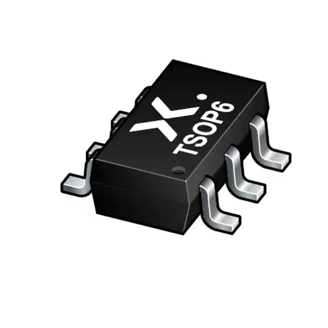
NPN/PNP low VCEsat transistor pair in a SOT457 (SC-74)
plastic package.
6, 3
collector
TR1; TR2
MARKING
TYPE NUMBER
PBSS4240DPN
6
handbook, halfpage
5
6
4
5
4
MARKING CODE
TR2
M3
TR1
1
Top view
Fig.1
2003 Feb 20
2
2
3
1
2
3
MAM445
Simplified outline SOT457 (SC-74) and
symbol.
�NXP Semiconductors
Product data sheet
40 V low VCEsat NPN/PNP transistor
PBSS4240DPN
LIMITING VALUES
In accordance with the Absolute Maximum Rating System (IEC 60134).
SYMBOL
PARAMETER
CONDITIONS
MIN.
MAX.
UNIT
Per transistor unless otherwise specified; for the PNP transistor with negative polarity
VCBO
collector-base voltage
open emitter
−
40
V
VCEO
collector-emitter voltage
open base
−
40
V
VEBO
emitter-base voltage
open collector
−
5
V
IC
collector current (DC)
−
NPN
−
1.35
A
PNP
−
−1.1
A
ICRP
repetitive peak collector current
note 1
−
2
A
ICM
peak collector current
single peak
−
3
A
IB
base current (DC)
−
300
mA
IBM
peak base current
−
1
A
Ptot
total power dissipation
Tamb ≤ 25 °C; note 2
−
370
mW
Tamb ≤ 25 °C; note 3
−
310
mW
Tamb ≤ 25 °C; note 1
−
1.1
W
Tstg
storage temperature
−65
+150
°C
Tj
junction temperature
−
150
°C
Tamb
operating ambient temperature
−65
+150
°C
−
600
mW
Per device
Ptot
total power dissipation
Tamb ≤ 25 °C; note 2
Notes
1. Operated under pulsed conditions: duty cycle δ ≤ 20%; pulse width tp ≤ 10 ms; mounting pad for collector standard
footprint.
2. Device mounted on a printed-circuit board; single-sided copper; tinplated; mounting pad for collector 1 cm2.
3. Device mounted on a printed-circuit board; single-sided copper; tinplated; standard footprint.
THERMAL CHARACTERISTICS
SYMBOL
PARAMETER
CONDITIONS
VALUE
UNIT
in free air; note 1
340
K/W
in free air; note 2
110
K/W
Per transistor
Rth j-a
thermal resistance from junction to
ambient
Notes
1. Device mounted on a printed-circuit board, single-sided copper, tinplated, mounting pad for collector 1 cm2.
2. Operated under pulsed conditions: pulse width tp ≤ 10 ms; duty cycle δ ≤ 0.20; mounting pad for collector standard
footprint.
2003 Feb 20
3
�NXP Semiconductors
Product data sheet
40 V low VCEsat NPN/PNP transistor
PBSS4240DPN
CHARACTERISTICS
Tamb = 25 °C unless otherwise specified.
SYMBOL
PARAMETER
CONDITIONS
MIN.
TYP.
MAX.
UNIT
Per transistor unless otherwise specified; for the PNP transistor with negative polarity
VCB = 40 V; IE = 0
−
−
100
nA
VCB = 40 V; IE = 0; Tj = 150 °C
−
−
50
μA
VCE = 30 V; IB = 0
−
−
100
nA
emitter-base cut-off current
VEB = 5 V; IC = 0
−
−
100
nA
hFE
DC current gain
VCE = 5 V; IC = 1 mA
300
−
−
fT
transition frequency
IC = 50 mA; VCE = 10 V;
f = 100 MHz
150
−
−
MHz
Cc
collector capacitance
VCB = 10 V; IE = Ie = 0;
f = 1 MHz
−
−
12
pF
DC current gain
VCE = 5 V; IC = 500 mA
300
−
900
VCE = 5 V; IC = 1 A
200
−
−
VCE = 5 V; IC = 2 A; note 1
75
−
−
IC = 100 mA; IB = 1 mA
−
60
75
mV
IC = 500 mA; IB = 50 mA
−
80
100
mV
IC = 1 A; IB = 100 mA
−
150
200
mV
IC = 2 A; IB = 200 mA; note 1
−
300
400
mV
ICBO
collector-base cut-off current
ICEO
collector-emitter cut-off current
IEBO
TR1 (NPN)
hFE
VCEsat
collector-emitter saturation voltage
VBEsat
base-emitter saturation voltage
IC = 1 A; IB = 100 mA
−
−
1.2
V
VBEon
base-emitter turn-on voltage
VCE = 5 V; IC = 1 A
−
−
1.1
V
RCEsat
equivalent on-resistance
IC = 1 A; IB = 100 mA
−
−
200
mΩ
DC current gain
VCE = −5 V; IC = −100 mA
300
−
800
VCE = −5 V; IC = −500 mA
250
−
−
VCE = −5 V; IC = −1 A
160
−
−
VCE = −5 V; IC = −2 A; note 1
50
−
−
IC = −100 mA; IB = −1 mA
−
−90
−120
mV
IC = −500 mA; IB = −50 mA
−
−100
−145
mV
IC = −1 A; IB = −100 mA
−
−180
−260
mV
IC = −2 A; IB = −200 mA; note 1
−
−400
−530
mV
TR2 (PNP)
hFE
VCEsat
saturation voltage
VBEsat
saturation voltage
IC = −1 A; IB = −50 mA
−
−
−1.1
V
VBEon
base-emitter turn-on voltage
VCE = −5 V; IC = −1 A
−
−
−1
V
RCEsat
equivalent on-resistance
IC = −1 A; IB = −100 mA; note 1
−
−
260
mΩ
Note
1. Pulse test: tp ≤ 300 μs; δ ≤ 0.02.
2003 Feb 20
4
�NXP Semiconductors
Product data sheet
40 V low VCEsat NPN/PNP transistor
PBSS4240DPN
MHC471
800
MHC472
1.2
handbook, halfpage
handbook, halfpage
hFE
VBE
(1)
(V)
600
(1)
0.8
(2)
(2)
400
(3)
0.4
(3)
200
0
10−1
1
10
102
0
10−1
103
104
IC (mA)
1
TR1 (NPN); VCE = 5 V.
(1) Tamb = 150 °C.
(2) Tamb = 25 °C.
(3) Tamb = −55 °C.
TR1 (NPN); VCE = 5 V.
(1) Tamb = −55 °C.
(2) Tamb = 25 °C.
(3) Tamb = 150 °C.
Fig.2
Fig.3
DC current gain as a function of collector
current; typical values.
MHC473
103
handbook, halfpage
10
102
103
104
IC (mA)
Base-emitter voltage as a function of
collector current; typical values.
MHC474
1.2
handbook, halfpage
VBEsat
(V)
VCEsat
(mV)
1
(1)
0.8
(2)
102
(1)
0.6
(2)
(3)
0.4
(3)
10
10−1
1
10
102
0.2
10−1
103
104
IC (mA)
1
TR1 (NPN); IC/IB = 20.
(1) Tamb = 150 °C.
(2) Tamb = 25 °C.
(3) Tamb = −55 °C.
TR1 (NPN); IC/IB = 20.
(1) Tamb = −55 °C.
(2) Tamb = 25 °C.
(3) Tamb = 150 °C.
Fig.4
Fig.5
Collector-emitter saturation voltage as a
function of collector current; typical values.
2003 Feb 20
5
10
102
103
104
IC (mA)
Base-emitter saturation voltage as a
function of collector current; typical values.
�NXP Semiconductors
Product data sheet
40 V low VCEsat NPN/PNP transistor
PBSS4240DPN
MHC475
2
IC
(A)
MHC476
103
handbook, halfpage
(1)
(2)
(3)
handbook, halfpage
RCEsat
(Ω)
(4)
(5)
(6)
1.6
102
(7)
1.2
(8)
(9)
10
(10)
0.8
1
0.4
(1)
10−1
10−1
0
0.8
0.4
0
1.2
1.6
2
VCE (V)
TR1 (NPN); Tamb = 25 °C.
(1)
(2)
(3)
(4)
IB = 30 mA.
IB = 27 mA.
IB = 24 mA.
IB = 21 mA.
(5) IB = 18 mA.
(9) IB = 6 mA.
(6) IB = 15 mA.
(7) IB = 12 mA.
(8) IB = 9 mA.
(10) IB = 3 mA.
Collector current as a function of
collector-emitter voltage; typical values.
2003 Feb 20
1
10
102
103
104
IC (mA)
TR1 (NPN); IC/IB = 20.
(1) Tamb = 150 °C.
(2) Tamb = 25 °C.
(3) Tamb = −55 °C.
Fig.7
Fig.6
(2)
(3)
6
Collector-emitter equivalent on-resistance
as a function of collector current; typical
values.
�NXP Semiconductors
Product data sheet
40 V low VCEsat NPN/PNP transistor
PBSS4240DPN
MHC464
1000
MHC465
−1.2
handbook, halfpage
handbook, halfpage
hFE
VBE
(V)
800
(1)
(1)
−0.8
(2)
600
(3)
(2)
400
−0.4
(3)
200
0
−10−1
−1
−10
−102
0
−10−1
−103
−104
IC (mA)
−1
TR2 (PNP); VCE = −5 V.
(1) Tamb = 150 °C.
(2) Tamb = 25 °C.
(3) Tamb = −55 °C.
TR2 (PNP); VCE = −5 V.
(1) Tamb = −55 °C.
(2) Tamb = 25 °C.
(3) Tamb = 150 °C.
Fig.8
Fig.9
DC current gain as a function of collector
current; typical values.
MHC466
−103
handbook, halfpage
−10
−102
−103
−104
IC (mA)
Base-emitter voltage as a function of
collector current; typical values.
MHC467
−1.2
handbook, halfpage
VBEsat
(V)
VCEsat
−1
(mV)
−102
(1)
−0.8
(1)
(2)
(2)
−0.6
(3)
−10
(3)
−0.4
−1
−10−1
−1
−10
−102
−0.2
−10−1
−103
−104
IC (mA)
TR2 (PNP); IC/IB = 20.
−1
−10
−102
−104
−103
IC (mA)
(1) Tamb = 150 °C.
(2) Tamb = 25 °C.
(3) Tamb = −55 °C.
TR2 (PNP); IC/IB = 20.
(1) Tamb = −55 °C.
(2) Tamb = 25 °C.
(3) Tamb = 150 °C.
Fig.10 Collector-emitter saturation voltage as a
function of collector current; typical values.
Fig.11 Base-emitter saturation voltage as a
function of collector current; typical values.
2003 Feb 20
7
�NXP Semiconductors
Product data sheet
40 V low VCEsat NPN/PNP transistor
PBSS4240DPN
MHC468
−1.2
MHC469
−2.4
IC
(A)
−2
handbook, halfpage
handbook, halfpage
IC
(A)
(4)
(3)
−0.8
(2)
(1)
(1)
(2)
(3)
(4)
(5)
−1.6
(5)
(6)
(7)
(8)
(6)
(7)
−1.2
(9)
(8)
−0.4
−0.8
(9)
(10)
0
0
−0.8
−0.4
−1.2
−0.4
0
−1.4
−2
VCE (V)
0
TR2 (PNP); Tamb = 25 °C.
(1)
(2)
(3)
(4)
IB = −7 mA.
IB = −6.3 mA.
IB = −5.6 mA.
IB = −4.9 mA.
(5) IB = −4.2 mA.
(6) IB = −3.5 mA.
(7) IB = −2.8 mA.
(8) IB = −2.1 mA.
−0.8
−0.4
−1.2
−1.6
−2
VCE (V)
TR2 (PNP); Tamb = 25 °C.
(9) IB = −1.4 mA.
(1)
(2)
(3)
(4)
(10) IB = −0.7 mA.
Fig.12 Collector current as a function of
collector-emitter voltage; typical values.
2003 Feb 20
(10)
IB = −50 mA.
IB = −45 mA.
IB = −40 mA.
IB = −35 mA.
(5) IB = −30 mA.
(6) IB = −25 mA.
(7) IB = −20 mA.
(8) IB = −15 mA.
(9) IB = −10 mA.
(10) IB = −5 mA.
Fig.13 Collector current as a function of
collector-emitter voltage; typical values.
8
�NXP Semiconductors
Product data sheet
40 V low VCEsat NPN/PNP transistor
PBSS4240DPN
MHC470
103
handbook, halfpage
RCEsat
(Ω)
102
10
(1)
(2)
1
(3)
10−1
−10−1
−1
−10
−102
−103
−104
IC (mA)
TR2 (PNP); IC/IB = 20.
(1) Tamb = 150 °C.
(2) Tamb = 25 °C.
(3) Tamb = −55 °C.
Fig.14 Collector-emitter equivalent on-resistance
as a function of collector current; typical
values.
2003 Feb 20
9
�NXP Semiconductors
Product data sheet
40 V low VCEsat NPN/PNP transistor
PBSS4240DPN
PACKAGE OUTLINE
Plastic surface mounted package; 6 leads
SOT457
D
E
B
y
A
HE
6
X
v M A
4
5
Q
pin 1
index
A
A1
c
1
2
3
Lp
bp
e
w M B
detail X
0
1
2 mm
scale
DIMENSIONS (mm are the original dimensions)
UNIT
A
A1
bp
c
D
E
e
HE
Lp
Q
v
w
y
mm
1.1
0.9
0.1
0.013
0.40
0.25
0.26
0.10
3.1
2.7
1.7
1.3
0.95
3.0
2.5
0.6
0.2
0.33
0.23
0.2
0.2
0.1
OUTLINE
VERSION
SOT457
2003 Feb 20
REFERENCES
IEC
JEDEC
EIAJ
SC-74
10
EUROPEAN
PROJECTION
ISSUE DATE
97-02-28
01-05-04
�NXP Semiconductors
Product data sheet
40 V low VCEsat NPN/PNP transistor
PBSS4240DPN
DATA SHEET STATUS
DOCUMENT
STATUS(1)
PRODUCT
STATUS(2)
DEFINITION
Objective data sheet
Development
This document contains data from the objective specification for product
development.
Preliminary data sheet
Qualification
This document contains data from the preliminary specification.
Product data sheet
Production
This document contains the product specification.
Notes
1. Please consult the most recently issued document before initiating or completing a design.
2. The product status of device(s) described in this document may have changed since this document was published
and may differ in case of multiple devices. The latest product status information is available on the Internet at
URL http://www.nxp.com.
the device. Limiting values are stress ratings only and
operation of the device at these or any other conditions
above those given in the Characteristics sections of this
document is not implied. Exposure to limiting values for
extended periods may affect device reliability.
DISCLAIMERS
General ⎯ Information in this document is believed to be
accurate and reliable. However, NXP Semiconductors
does not give any representations or warranties,
expressed or implied, as to the accuracy or completeness
of such information and shall have no liability for the
consequences of use of such information.
Terms and conditions of sale ⎯ NXP Semiconductors
products are sold subject to the general terms and
conditions of commercial sale, as published at
http://www.nxp.com/profile/terms, including those
pertaining to warranty, intellectual property rights
infringement and limitation of liability, unless explicitly
otherwise agreed to in writing by NXP Semiconductors. In
case of any inconsistency or conflict between information
in this document and such terms and conditions, the latter
will prevail.
Right to make changes ⎯ NXP Semiconductors
reserves the right to make changes to information
published in this document, including without limitation
specifications and product descriptions, at any time and
without notice. This document supersedes and replaces all
information supplied prior to the publication hereof.
Suitability for use ⎯ NXP Semiconductors products are
not designed, authorized or warranted to be suitable for
use in medical, military, aircraft, space or life support
equipment, nor in applications where failure or malfunction
of an NXP Semiconductors product can reasonably be
expected to result in personal injury, death or severe
property or environmental damage. NXP Semiconductors
accepts no liability for inclusion and/or use of NXP
Semiconductors products in such equipment or
applications and therefore such inclusion and/or use is at
the customer’s own risk.
No offer to sell or license ⎯ Nothing in this document
may be interpreted or construed as an offer to sell products
that is open for acceptance or the grant, conveyance or
implication of any license under any copyrights, patents or
other industrial or intellectual property rights.
Export control ⎯ This document as well as the item(s)
described herein may be subject to export control
regulations. Export might require a prior authorization from
national authorities.
Applications ⎯ Applications that are described herein for
any of these products are for illustrative purposes only.
NXP Semiconductors makes no representation or
warranty that such applications will be suitable for the
specified use without further testing or modification.
Quick reference data ⎯ The Quick reference data is an
extract of the product data given in the Limiting values and
Characteristics sections of this document, and as such is
not complete, exhaustive or legally binding.
Limiting values ⎯ Stress above one or more limiting
values (as defined in the Absolute Maximum Ratings
System of IEC 60134) may cause permanent damage to
2003 Feb 20
11
�NXP Semiconductors
Customer notification
This data sheet was changed to reflect the new company name NXP Semiconductors. No changes were
made to the content, except for the legal definitions and disclaimers.
Contact information
For additional information please visit: http://www.nxp.com
For sales offices addresses send e-mail to: salesaddresses@nxp.com
© NXP B.V. 2009
All rights are reserved. Reproduction in whole or in part is prohibited without the prior written consent of the copyright owner.
The information presented in this document does not form part of any quotation or contract, is believed to be accurate and reliable and may be changed
without notice. No liability will be accepted by the publisher for any consequence of its use. Publication thereof does not convey nor imply any license
under patent- or other industrial or intellectual property rights.
Printed in The Netherlands
613514/01/pp12
Date of release: 2003 Feb 20
Document order number: 9397 750 10783
�