物料型号:PESD3V3S4UF 和 PESD5V0S4UF
器件简介:
- 这些是单向四路 ESD 保护二极管阵列,设计用于保护多达四条信号线免受静电放电(ESD)和其他瞬态现象引起的损害。
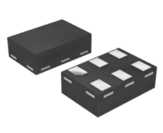
它们采用小型的 SOT886 表面贴装设备(SMD)塑料封装。
引脚分配:
- 引脚1:二极管1的阴极
- 引脚2:公共阳极
- 引脚3:二极管2的阴极
- 引脚4:二极管3的阴极
- 引脚5:公共阳极
- 引脚6:二极管4的阴极
参数特性:
- PESD3V3S4UF 反向工作电压(VRWM):3.3V
- PESD5V0S4UF 反向工作电压(VRWM):5.0V
- PESD3V3S4UF 二极管电容(Cd,1MHz):110pF 至 300pF
- PESD5V0S4UF 二极管电容(Cd,1MHz):85pF 至 220pF
功能详解:
- 这些器件提供了高达 30kV 的 ESD 保护,符合 IEC 61000-4-2 标准第 4 级(ESD),以及 IEC 61000-4-5(浪涌)标准,其中冲击脉冲功率(IPP)为 10A。
它们还通过了 AEC-Q101 认证。
应用信息:
- 适用于计算机和外围设备、通信系统、便携式电子设备、音视频设备、手机及其配件。
封装信息:
- PESD3V3S4UF 和 PESD5V0S4UF 都采用 SOT886 封装,这是一种塑料极薄小型外型封装,无引线,6 个端子,封装尺寸为 1x1.45x0.5 mm。
以上信息摘自 Nexperia 的产品数据表,修订日期为 2008 年 1 月 17 日。