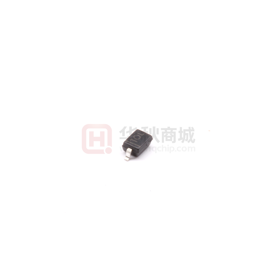
ESD56151WXX
ESD56151WXX
1-Line, Bi-directional, Transient Voltage Suppressor
http//:www.sh-willsemi.com
Descriptions
The ESD56151WXX is a transient voltage suppressor
designed to protect power interfaces. It is suitable to replace
multiple discrete components in portable electronics.
The ESD56151WXX is specifically designed to protect power
lines.
SOD-323
The ESD56151WXX is available in SOD-323 package.
Standard products are Pb-free and Halogen-free.
Pin1
Features
Reverse stand-off voltage: 4.5V ~ 5V
Surge protection according to IEC61000-4-5
Circuit diagram
see Table 4
Pin2
ESD protection according to IEC61000-4-2
±30kV (contact and air discharge)
Low clamping voltage
Solid-state silicon technology
Applications
X= Device code (O P)
Power supply protection
* = Month code
Power management
Marking (Top View)
Order information
Table 1.
Device
Package
Shipping
Marking
ESD56151W04-2/TR
SOD-323
3000/Tape&Reel
TO*
ESD56151W05-2/TR
SOD-323
3000/Tape&Reel
TP*
Will Semiconductor Ltd.
1
Revision 1.0, 2017/04/18
�ESD56151WXX
Absolute maximum ratings
Table 2.
Parameter
Peak pulse power (tp = 8/20μs)
ESD according to IEC61000-4-2 air discharge
Symbol
Rating
Unit
Ppk
2400
W
VESD
ESD according to IEC61000-4-2 contact discharge
Junction temperature
TJ
Operating temperature
TOP
Lead temperature
TL
Storage temperature
TSTG
±30
kV
±30
125
o
-40~85
o
260
o
-55~150
o
C
C
C
C
Electrical characteristics (TA = 25oC, unless otherwise noted)
I
VRWM Reverse stand-off voltage
IR
Reverse leakage current
VCL
Clamping voltage
IPP
Peak pulse current
IPP
IHOLD
VHOLD
VCL VTRIG
VRWM
ITRIG
IR
IR
ITRIG
VRWM VTRIG
VHOLD
VCL
V
IHOLD
VTRIG Reverse trigger voltage
ITRIG
Reverse trigger current
VHOLD Reverse holding voltage
IHOLD
IPP
Reverse holding current
Definitions of electrical characteristics
Will Semiconductor Ltd.
2
Revision 1.0, 2017/04/18
�ESD56151WXX
o
Electrical characteristics (TA = 25 C, unless otherwise noted)
Table 3.
Reverse
Stand-off
Type number
Breakdown voltage
Voltage
VBR(V)
IBR = 1mA
VRWM (V)
Junction
Reverse
leakage current
IRM(μA) at VRWM
capacitance
F = 1MHz,
VR=0V (pF)
Max.
Min.
Typ.
Max.
Typ.
Max.
Typ.
Max.
ESD56151W04
4.5
4.7
5.3
6.4
-
0.1
280
350
ESD56151W05
5.0
5.3
6.3
7.1
-
0.1
400
450
Table 4.
Type number
Rated peak pulse
current IPP (A)
1)3)
Clamping voltage
VCL(V) at IPP(A)
1)3)
Clamping voltage
VCL(V) at
IPP = 16A,
tp = 100ns
2)3)
Clamping voltage
VCL(V) at
VESD = 8kV
ESD56151W04
150
16
6.5
7.0
ESD56151W05
145
16
6.7
7.5
2)3)
Notes:
1)
Non-repetitive current pulse, according to IEC61000-4-5. (8/20μs current waveform)
2)
Non-repetitive current pulse, according to IEC61000-4-2.
3)
Measured from pin 1 to pin 2.
Will Semiconductor Ltd.
3
Revision 1.0, 2017/04/18
�ESD56151WXX
o
Electrical characteristics (TA = 25 C, unless otherwise noted)
100
90
Time to half-value: T2= 20μs
Current (%)
Peak pulse current (%)
100
90
Front time: T1= 1.25 T = 8μs
50
T2
10
10
0
0
T
5
10
T1
15
Time (μs)
20
25
14
12
ESD56151W05
ESD56151W04
8
6
4
0
25
50
75
100
500
CJ - Junction capacitance (pF)
VC - Clamping voltage (V)
Pulse waveform: tp = 8/20s
10
125
f = 1MHz
VAC = 50mV
400
300
ESD56151W05
200
ESD56151W04
100
0
150
0
1
IPP - Peak pulse current (A)
3
4
5
6
Capacitance vs. Reverse voltage
100
% of Rated power
10
Peak pulse power (kW)
2
VR - Reverse voltage (V)
Clamping voltage vs. Peak pulse current
1
0.1
Time (ns)
Contact discharge current waveform per IEC61000-4-2
8/20μs waveform per IEC61000-4-5
16
tr = 0.7~1ns
t
60ns
30ns
30
1
10
100
Pulse time (s)
60
40
20
0
1000
0
25
50
75
100
125
150
o
TA - Ambient temperature ( C)
Non-repetitive peak pulse power vs. Pulse time
Will Semiconductor Ltd.
80
Power derating vs. Ambient temperature
4
Revision 1.0, 2017/04/18
�ESD56151WXX
PACKAGE OUTLINE DIMENSIONS
SOD-323
D
A2
A1
b
E
D1
A
Side View
L1
L
c
θ
Top View
Side View
Dimensions in Millimeters
Symbol
Min.
Typ.
Max.
A
0.800
-
1.100
A1
0.800
0.850
0.900
A2
0.000
-
0.100
b
0.250
-
0.400
c
0.080
-
0.177
D1
1.600
1.700
1.800
D
2.300
-
2.800
E
1.150
-
1.400
L
0.475 Ref.
L1
0.100
-
0.500
θ
0°
-
8°
Recommended land pattern (Unit: mm)
0.80
1.40
Notes:
0.80
This recommended land pattern is for reference
purposes only. Please consult your manufacturing
group to ensure your PCB design guidelines are met.
Will Semiconductor Ltd.
5
Revision 1.0, 2017/04/18
�ESD56151WXX
TAPE AND REEL INFORMATION
RD
Reel Dimensions
W
Tape Dimensions
P1
Quadrant Assignments For PIN1 Orientation In Tape
Q1
Q2
Q1
Q2
Q3
Q4
Q3
Q4
RD
Reel Dimension
W
Overall width of the carrier tape
P1
Pitch between successive cavity centers
Pin1
Pin1 Quadrant
Will Semiconductor Ltd.
User Direction of Feed
7inch
13inch
1 8mm
12mm
16mm
2mm
4mm
8mm
Q1
Q2
Q3
6
Q4
Revision 1.0, 2017/04/18
�
很抱歉,暂时无法提供与“ESD56151W04-2/TR”相匹配的价格&库存,您可以联系我们找货
免费人工找货- 国内价格
- 10+0.56565
- 100+0.46983
- 600+0.40020
- 1200+0.39420
- 3000+0.38237
- 国内价格
- 1+0.37620
- 200+0.24200
- 1500+0.21120
- 3000+0.18700
- 国内价格
- 10+0.67878
- 100+0.55761
- 300+0.46980
- 1000+0.39734
- 国内价格
- 20+0.81930
- 100+0.48870
- 800+0.34210
- 3000+0.24440
- 6000+0.23220
- 30000+0.21500
