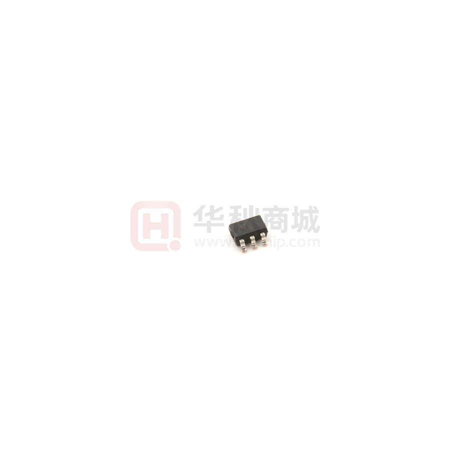
ESDA6V1W5
ESDA6V1W5
4-Lines, Uni-directional, Transient Voltage Suppressors
http//:www.sh-willsemi.com
Descriptions
The ESDA6V1W5 array is 4-line ESD transient voltage
suppressor which provides a very high level of protection for
sensitive electronic components that may be subjected to
electrostatic discharge (ESD). These devices clamp the
voltage just above the logic level supply for positive transient
SOT-353
and to a diode drop below ground for negative transient.
The ESDA6V1W5 may be used to provide ESD protection up
to ±30kV (contact discharge) according to IEC61000-4-2,
and withstand peak pulse current up to 9A (8/20μs)
1
5
2
according to IEC61000-4-5.
The ESDA6V1W5 is available in SOT-353 package.
3
4
Standard products are Pb-free and Halogen-free.
Features
Circuit diagram
Reverse stand-off voltage: 5V max.
Transient pr6otection for each line according to
IEC61000-4-2 (ESD):
I/O
I/O
5
4
±30kV (contact discharge)
IEC61000-4-5 (surge): 9A (8/20μs)
Capacitance: CJ = 55pF typ.
Low leakage current
Low clamping voltage
Solid-state silicon technology
*E
Applications
Cell Phone Handsets and Accessories
Personal Digital Assistants
Notebooks, Desktops, and Servers
Portable Instrument
1
2
3
I/O
GND
I/O
E
*
= Device code
= Date code
Marking & Pin configuration
Order information
Device
Package
Shipping
ESDA6V1W5-5/TR SOT-353 3000/Tape&Reel
Will Semiconductor Ltd.
1
Revision 3.3, 2016/03/28
�ESDA6V1W5
Absolute maximum ratings
Parameter
Symbol
Rating
Unit
Peak pulse power (tp = 8/20μs)
Ppk
117
W
Peak pulse current (tp = 8/20μs)
IPP
9
A
ESD according to IEC61000-4-2 air discharge
±30
VESD
ESD according to IEC61000-4-2 contact discharge
Junction temperature
±30
TJ
Operation temperature
TOP
Lead temperature
TL
Storage temperature
TSTG
kV
125
o
-40~85
o
260
o
-55~150
o
C
C
C
C
Electrical characteristics (TA = 25oC, unless otherwise noted)
I
IPP
VF
Forward voltage
VRWM Reverse stand-off voltage
IF
Forward current
IR
Reverse leakage current
VFC
Forward clamping voltage
VBR
Reverse breakdown voltage
IPP
Peak pulse current
VCL
Clamping voltage
IPP
Peak pulse current
VFC VF
IBR
IR
VRWM VBR VCL
V
IF
IPP
Definitions of electrical characteristics
Will Semiconductor Ltd.
2
Revision 3.3, 2016/03/28
�ESDA6V1W5
o
Electrical characteristics (TA = 25 C, unless otherwise noted)
Parameter
Symbol
Condition
Min.
Typ.
Max.
Unit
5.0
V
1
μA
Reverse stand-off voltage
VRWM
Reverse leakage current
IR
VRWM = 5V
Reverse breakdown voltage
VBR
IBR = 1mA
6.2
7.2
8.2
V
Forward voltage
VF
IF = 10mA
0.4
0.8
1.25
V
VCL
IPP = 16A, tp = 100ns
11.0
V
VCL
VESD = +8kV
11.0
V
0.25
Ω
1)
Clamping voltage
Clamping voltage
2)
Dynamic resistance
Clamping voltage
1)
3)
Junction capacitance
RDYN
VCL
CJ
IPP = 1A, tp = 8/20μs
9
V
IPP = 9A, tp = 8/20μs
13
V
65
pF
VR = 0V, f = 1MHz
55
Notes:
1) TLP parameter: Z0 = 50 Ω, tp = 100ns, tr = 2ns, averaging window from 60ns to 80ns. RDYN is calculated from 4A to
16A.
2) Contact discharge mode, according to IEC61000-4-2
3)
Non-repetitive current pulse, according to IEC61000-4-5.
Will Semiconductor Ltd.
3
Revision 3.3, 2016/03/28
�ESDA6V1W5
o
100
90
Front time: T1= 1.25 T = 8μs
100
90
Time to half-value: T2= 20μs
Current (%)
Peak pulse current (%)
Typical characteristics (TA = 25 C, unless otherwise noted)
50
T2
10
10
0
tr = 0.7~1ns
Time (μs)
T1
8/20μs waveform per IEC61000-4-5
t
60ns
30ns
20
T
Time (ns)
Contact discharge current waveform per IEC61000-4-2
10.5
Junction capacitance (pF)
VC - Clamping voltage (V)
Pulse waveform: tp = 8/20μs
10.0
9.5
9.0
8.5
8.0
f = 1MHz
VAC = 50mV
50
45
40
35
30
7.5
7.0
55
0
1
2
3
4
5
6
7
8
9
25
10
0
1
IPP - Peak pulse current (A)
2
3
4
5
VR - Reverse voltage (V)
Clamping voltage vs. Peak pulse current
Capacitance vs. Reverse voltage
1000
% of Rated power
Peak pulse power (W)
100
100
10
80
60
40
20
0
1
10
100
Pulse time (μs)
1000
25
50
75
100
125
150
o
TA - Ambient temperature ( C)
Non-repetitive peak pulse power vs. Pulse time
Will Semiconductor Ltd.
0
Power derating vs. Ambient temperature
4
Revision 3.3, 2016/03/28
�ESDA6V1W5
o
Typical characteristics (TA = 25 C, unless otherwise noted)
10V/div
TLP current (A)
10V/div
22
20
18
16
14
12
10
8
6
4
2
0
-2
20ns/div
20ns/div
ESD clamping
ESD clamping
(+8kV contact discharge per IEC61000-4-2)
(-8kV contact discharge per IEC61000-4-2)
Z0 = 50
tr = 2ns
tp = 100ns
0
1
2
3
4
5
6
7
8
9
10 11 12
TLP voltage (V)
TLP Measurement
Will Semiconductor Ltd.
5
Revision 3.3, 2016/03/28
�ESDA6V1W5
Package outline dimensions
SOT-353
D
e1
θ
L1
E
E1
L
e
C
b
A1
0.2
Recommend land pattern (Unit: mm)
0.40
Dimensions in Millimeters
Min.
Typ.
Max.
A
0.850
-
1.050
A1
0.000
-
0.100
A2
0.800
0.900
1.000
b
0.150
0.250
0.350
c
0.008
-
0.150
D
2.000
2.100
2.200
E
1.150
1.250
1.350
E1
2.150
2.300
2.450
A
A2
Symbol
0.65
0.80
e
e1
0.650 TYP
1.200
1.94
L
1.300
1.400
0.525 REF
L1
0.260
0.360
0.460
θ
0°
-
8°
Notes:
This recommended land pattern is for reference
purposes only. Please consult your manufacturing
group to ensure your PCB design guidelines are met.
1.30
Will Semiconductor Ltd.
6
Revision 3.3, 2016/03/28
�
很抱歉,暂时无法提供与“ESDA6V1W5-5/TR”相匹配的价格&库存,您可以联系我们找货
免费人工找货- 国内价格
- 20+0.58330
- 100+0.34800
- 800+0.24360
- 3000+0.17400
- 6000+0.16530
- 30000+0.15310
- 国内价格
- 10+0.28910
- 100+0.25588
