Thyristor Surge Suppressors
P0060~P3500SA_B_C Serise
Description
P0060~P3500SA_B_C Series are low capacitance devices
designed to protect broadband equipment such as VOIP,
DSL modems and DSLAMs from damaging overvoltage
transients.
The series provides a surface mount solution that enables
equipment to comply with global regulatory standards while
limiting the impact to broadband signals.
Features and Benefits
• Low voltagr overeshoot
• Low on-state voltage
• Does not degrade with use
• Fails short circuit when surged in excess of ratings
• Low Capacitance
Applicable Global Standards
• TIA-968-A
• ITU K.20/21 Enhanced level*
• ITU K.20/21 Basic Level
• GR 1089 Inter building*
• GR 1089 Inter building
• IEC 6100-4-5
• YD/T 1082
• YD/T 993
• YD/T 950
Product Name
P
Logo
0
0
Vdrm
8
0
0:Represents a
chip
S
B
Type
S:SMD SMB
T:SMD SMA
E:DIP TO-92
L:DIP D0-15
All data is subject to change,Please check our data sheets at www ruilon com for updates.
Peak pilse
current-Ipp
8/20μs
A=150A
B=250A
C=400A
©2012 RuiLong Yuan,Inc.
TSS 01
�Electriacl Characteristics (@ TA = 25 °C Unless Otherwise Noted)
Type Number
VDRM
IDRM
VBO
IH
IS
IT
VT
CJ
V
μA
V
MA
MA
A
V
pFMin
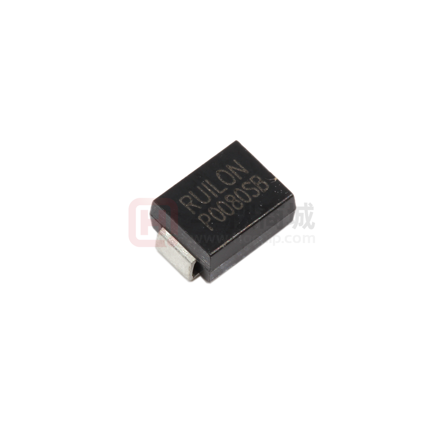
P0080SA
6
5
25
50
800
2.2
4
25
150
P0080SB
6
5
25
50
800
2.2
4
25
150
pFMax
P0080SC
6
5
25
50
800
2.2
4
35
260
P0300SA
25
5
40
50
800
2.2
4
15
140
P0300SB
25
5
40
50
800
2.2
4
15
140
P0300SC
25
5
40
50
800
2.2
4
25
250
P0640SA
58
5
77
150
800
2.2
4
40
60
P0640SB
58
5
77
150
800
2.2
4
40
60
155
P0640SC
58
5
77
150
800
2.2
4
55
P0720SA
65
5
88
150
800
2.2
4
35
60
P0720SB
65
5
88
150
800
2.2
4
35
75
150
P0720SC
65
5
88
150
800
2.2
4
50
P0900SA
75
5
98
150
800
2.2
4
35
55
P0900SB
75
5
98
150
800
2.2
4
35
70
140
P0900SC
75
5
98
150
800
2.2
4
45
P1100SA
90
5
130
150
800
2.2
4
30
50
P1100SB
90
5
130
150
800
2.2
4
30
70
115
P1100SC
90
5
130
150
800
2.2
4
45
P1300SA
120
5
160
150
800
2.2
4
25
45
P1300SB
120
5
160
150
800
2.2
4
25
60
105
P1300SC
120
5
160
150
800
2.2
4
40
P1500SA
140
5
180
150
800
2.2
4
25
40
P1500SB
140
5
180
150
800
2.2
4
25
55
P1500SC
140
5
180
150
800
2.2
4
35
95
P1800SA
170
5
220
150
800
2.2
4
25
35
P1800SB
170
5
220
150
800
2.2
4
25
50
P1800SC
170
5
220
150
800
2.2
4
35
90
P2300SA
190
5
260
150
800
2.2
4
25
35
P2300SB
190
5
260
150
800
2.2
4
25
50
P2300SC
190
5
260
150
800
2.2
4
30
80
P2600SA
220
5
300
150
800
2.2
4
20
35
P2600SB
220
5
300
150
800
2.2
4
20
45
P2600SC
220
5
300
150
800
2.2
4
30
80
P3100SA
275
5
350
150
800
2.2
4
20
35
P3100SB
275
5
350
150
800
2.2
4
20
45
70
P3100SC
275
5
350
150
800
2.2
4
30
P3500SA
320
5
400
150
800
2.2
4
20
35
P3500SB
320
5
400
150
800
2.2
4
20
40
P3500SC
320
5
400
150
800
2.2
4
25
65
Package Dimensions
inch(mm)
Notes:
- Absolute maximum ratings measured at TA= 25ºC (unless otherwise noted).
- Devices are bi-directional.
SERIES
TSS 02
Peak Pilse Current-lpp(A)
10/160µs
10/560µs
2/10µs
8/20µs
A
200
150
100
60
50
B
250
250
150
100
80
C
500
400
200
120
100
All data is subject to change,Please check our data sheets at www ruilon com for updates.
10/1000µs
©2012 RuiLong Yuan,Inc.
�Surge Ratings
IPP
Series
ITSM
50/60 Hz
di/dt
2x10 µs
8x20 µs
10x160 µs
10x560 µs
10x1000 µs
A min
A min
A min
A min
A min
A min
A/μs max
A
150
150
90
50
45
20
500
B
250
250
150
100
80
30
500
C
500
400
200
150
100
50
500
Notes:
1 Current waveform in µs
2 Voltage waveform in µs
- Peak pulse current rating (IPP) is repetitive and guaranteed for the life of the product.
- IPP
- The device must initially be in thermal equilibrium with -40°C < TJ <
Thermal Considerations
Package
Symbol
DO-214AA
Parameter
Value
Unit
TJ
Operating Junction Temperature Range
°C
TS
Storage Temperature Range
°C
R0JA
Thermal Resistance: Junction to Ambient
V-I Characteristics
90
°C/W
t r x t d Pulse Waveform
IPP – Peak Pulse Current – %I PP
+I
IT
IS
IH
IDRM
-V
+V
VT
VDRM
VS
tr = rise time to peak v alue
td = decay time to half value
Peak
Value
100
Waveform = t r x td
50
Half Value
0
0
td
tr
t – Time (µs)
-I
S
Change vs. Junction Temperature
Normalized DC Holding Current vs. Case Temperature
14
12
10
IH
8
6
25 °C
4
2
0
-4
-6
-8
IH (TC = 25ºC)
2.0
Ratio of
Percent of V S Change – %
Normalized V
1.8
1.6
1.4
1.0
0.8
0.6
0.4
-40 -20
0
20 40 60 80 100 120 140 160
Junction Temperature (T
J)
25°C
1.2
-40
-20
– °C
All data is subject to change,Please check our data sheets at www ruilon com for updates.
0
20
40
60
80
100 120 140
160
Case Temperature (T C) - ºC
©2012 RuiLong Yuan,Inc.
TSS 03
�Figure 1.E
xamples of protection stages for line cards
Line
Protection stage
Protection stage
Ring
relay
Line
Ex . A n al o g l i n e c ar d
Ex . x DSL l i n e c ar d o r t er m i n al
In such a stage, parallel function is assumed by one or several Trisil, and is used to protect
against short duration surge (lightning). During this kind of surges the Trisil limits the voltage
across the device to be protected at its break over value and then fires. The fuse assumes
the series function, and is used to protect the module against long duration or very high
current mains disturbances (50/60Hz). It acts by safe circuit opening. Lightning surge and
mains disturbance surges are defined by standards like GR1089, FCC part 68, ITU-T K20.
Figure 2. Typical circuits
Fuse TCP 1.25A
Tip L
Tip S
Gnd
Gnd
Fuse TCP 1.25A
T1
T2
Fuse TCP 1.25A
Ring S
Ring L
Typical circuit for subscriber side
Typical circuit for central office side
Figure 3.T est circuit 1 for Dynamic I BO and V BO parameters
100V/µ s, di /dt< 10 A/ µs, Ipp= XXXA
2
U
83
45
10 µF
66
46 µH
0.36 nF
470
KeyTek 'System 2' generatorw ithP N246I module
1k V/ µs, di /dt< 10 A/ µs, Ipp= 10 A
26 µH
U
60 µF
250
47
46 µH
12
KeyTek 'System 2' generatorw ithP N246I module
TSS 04
All data is subject to change,Please check our data sheets at www ruilon com for updates.
©2012 RuiLong Yuan,Inc.
�Figure 5. Test circuit 3 for dynamic I H parameter
R
Surge generator
D.U.T
VBAT =- 48 V
This is a GO-NOGO test which allows to confirm the holding current (IH) level in a
functional test circuit.
TEST PROCEDURE
1/ Adjust the current level at the Iv Halue by short circuiting the AK of the D.U.T.
2/ Fire the D.U.T.w ith a surge current
I=
PP 10A, 10/1000µs.
3/ The D.U.T.w ill come back off-state within 50ms maximum.
Figure 4. Test circuit 2 for I BO and V BO parameters
K
ton = 20ms
R1 = 140
R2 = 240
220V 50Hz
DUT
Vout
VBO
measurement
1/4
IBO
measurement
TEST PROCEDURE
Pulse test duration (tp = 20ms):
for Bidirectional devices = Switch K is closed
for Unidirectional devices = Switch K is open
VOUT selection:
Device with V<
BO
Device with VBO
200VV
200VV
OUTR=
OUTR=
250V MS, R1 = 140
480V MS, R2 = 240
All data is subject to change,Please check our data sheets at www ruilon com for updates.
©2012 RuiLong Yuan,Inc.
TSS 05
�Soldering Parameters
Pb-Free assembly
(see Fig. 1)
Pre Heat
- Temperature Max (T
s(min)
TP
)
s(max)
- Time (Min to Max) (t s)
Average ramp up rate (Liquidus Temp (T
to peak)
60-180 secs.
)
L
TS(max) to TL - Ramp-up Rate
3°C/sec. Max.
3°C/sec. Max.
- Temperature (T L) (Liquidus)
- Temperature (t L)
60-150 secs.
Peak Temp (T P)
30 secs. Max.
Ramp-down Rate
6°C/sec. Max.
Time 2 5°C to Peak Temp (T P)
8 min. Max.
Critical Zone
TL to T P
TL
TS(max)
tL
Ramp-down
Preheat
TS(min)
25
Time within 5°C of actual Peak Temp (t p)
tP
Ramp-up
)
Tem p er at u re
- Temperature Min (T
Figure 1
tS
time to peak temperature
(t 2 5ºC to peak)
Time
Do not exceed
Lead Material
Copper Alloy
Terminal Finish
100% Matte-Tin Plated
Body Material
High Temp Voltage
Blocking
80% Rated VDRM (VAC Peak
504 or 1008 hrs. MIL-STD-750 (Method 1040)
JEDEC, JESD22-A-101
Temp Cycling
cycles. MIL-STD-750 (Method 1051) EIA/JEDEC,
JESD22-A104
Biased Temp &
Humidity
52 VDC
JEDEC, JESD22-A-101
High Temp Storage
JEDEC, JESD22-A-101
Low Temp Storage
-65°C, 1008 hrs.
Thermal Shock
10 cycles. MIL-STD-750 (Method 1056) JEDEC,
JESD22-A-106
Autoclave (Pressure
Cooker Test)
JEDEC, JESD22-A-102
Resistance to Solder
Heat
Moisture Sensitivity
Level
TSS 06
All data is subject to change,Please check our data sheets at www ruilon com for updates.
©2012 RuiLong Yuan,Inc.
�Dimensions — DO-214AA
Pad Outline
Case
Temperature
Measurement
Point
B
D
0.110
(2.8)
C A
0.079
(2.0)
H
E
inch
(millimeter)
F
K
Inches
Dimensions
0.079
(2.0)
G
Part Numbering
Min
Millimeters
Max
Min
Max
A
0.130
0.156
3.30
B
0.201
0.220
5.10
3.95
5.60
C
0.077
0.087
1.95
2.20
4.60
D
0.159
0.181
4.05
E
0.030
0.063
0.75
1.60
F
0.075
0.096
1.90
2.45
G
0.002
0.008
0.05
0.20
H
0.077
0.104
1.95
2.65
K
0.006
0.016
0.15
0.41
Part Marking
P xxx 0 S C
TYPE
P = LOGO
Pxxxx
Part Marking Code
(Refer to Electrical Characteristics Table)
MEDIAN VOLTAGE
CONSTRUCTION VARIABLE
IPP RATING
PACKAGE TYPE
Packing Options
Industry Standard
S
DO-214AA
Tape & Reel Pack
2500
N/A
EIA-481-D
0.157
(4.0)
0.472
(12.0)
0.36
(9.2)
0.315
(8.0)
0.059 DIA
(1.5)
12.99
(330.0)
0.512 (13.0)
Arbor Hole Dia.
0.49
(12.4)
Cover tape
Dimensions are in inches
(and millimeters).
Direction of Feed
All data is subject to change,Please check our data sheets at www ruilon com for updates.
©2012 RuiLong Yuan,Inc.
TSS 07
�RUILONG.YUAN CO.,LTD
Tel: +86- 0755-82908296
Fax: +86- 0755-82908002
Email: jack@ruilon.com
Website: http://www.ruilon.com
RuiLongYuan Electronics are trademarks.
Information furnished is believed to be accurate and reliable. However, users should independently evaluate the suitability of and test each
product selected for their own applications. RUILONYUAN Electronics reserves the right to change or update, without notice, any information
contained in this publication; to change, without notice, the design, construction, processing, or specification of any product; and to discontinue
or limit production or distribution of any product. This publication supersedes and replaces all information previously supplied. Without
expressed or written consent by an officer of RUILONYUAN Electronics, RUILONYUAN Electronics does not authorize the use of any of its
products as components in nuclear facility applications, aerospace, or in critical life support devices or systems. RUILONYUAN Electronics
expressly disclaims all implied warranties regarding the information contained herein, including, but not limited to, any implied warranties of
merchantability or fitness for a particular purpose. RUILONYUAN Electronics’ only obligations are those in the RUILONYUAN Electronics
Standard Terms and Conditions of Sale and in no case will RUILONYUAN Electronics be liable for any incidental, indirect, or consequential
damages.
TSS 08
All data is subject to change,Please check our data sheets at www ruilon com for updates.
©2012 RuiLong Yuan,Inc.
�