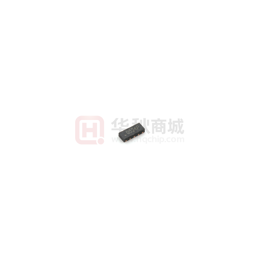
ESD0524P
Ultra Low Capacitance ESD Protection Array
DFN2510 Plastic-Encapsulate Diodes
DESCRIPTION
ESD0524P is an ultra-low capacitance Transient Voltage Suppressor (TVS) designed to protection for
high-speed data interfaces. With typical capacitance of 0.2pF (I/O to I/O) only, ESD0524P is designed
to protect parasitic-sensitive systems against over-voltage and over-current transient events. It
complies with IEC 61000-4-2 (ESD), Level 4(±15KV air, ±8KV contact discharge), IEC61000-4-4
(electrical fast transient-EFT) (40A, 5/50ns),very fast charged device model (CDM) ESD and cable
discharge event(CDE), etc.
ESD0524P uses ultra-small DFN2510 package. Each ESD0524P device can protect four high-speed
data lines. The combined features of ultra-low capacitance, ultra-small size and high ESD robustness
make ESD0524P ideal for high-speed data ports and high-frequency lines (e.g., HDMI &DVI)
applications. The low clamping voltage of the ESD0524P guarantees a minimum stress on the
protected IC.
Features
Mechanical Characteristics
Transient protection for asymmetrical data lines
IEC61000-4-2 (ESD) ±25kV (air), ±20kV (contact)
IEC61000-4-4 (EFT) 40A (5/50ns)
Cable Discharge Event(CDE)
Package optimized for high-speed lines
Protects four data lines
Low capacitance:0.2pF ( I/O to I/O)
Low leakage current
Low clamping voltage
Each I/O pin can withstand over 1000 ESD
strikes for ±8KV contact discharge
Package: DFN2510
Flammability Rating: UL 94V-0
Terminal: Matte tin plated.
High temperature soldering guaranted:
260℃/10s
Marking: 0524P
Packaging: Tape and Reel
Applications
Serial ATA
MDDI Ports
High Definition Multi-Media Interface (HDMI)
Desktops, Servers and Notebooks
Display Ports
USB 2.0/3.0 Power and Data Line Protection
Digital Visual Interface (DVI)
Package Outline & Pin Configuration
10
9
8
7
6
1
2
3
4
5
Pin
Identification
1,2,4,5
Input Lines
3,8
Ground
6 , 7 , 9 , 10
Output Lines
(No Internal Connection)
PCI Express
Circuit Diagram
Pin 1
Pin 2
Pin 4
Pin 5
3, 8
DN:T20427A0
http://www.microdiode.com
Rev:2020A0
Page :1
�ESD0524P
Ultra Low Capacitance ESD Protection Array
Absolute Maximum Ratings (TA=25°C unless otherwise specified)
Symbol
Parameter
Value
Units
PPP
Peak Pulse Power (8/20μs)
60
W
VESD
ESD per IEC 61000-4-2 (Air)
ESD per IEC 61000-4-2 (Contact)
±25
±20
kV
TOPT
Operating Temperature
-55/+125
C
TSTG
Storage Temperature
-55/+150
C
Electrical Characteristics (TA=25°C unless otherwise specified)
Symbol
Parameter
Test Condition
VRWM
Reverse Working Voltage
Any I/O pin to GND
VBR
Reverse Breakdown
Voltage
IR
Reverse Leakage Current
IT = 1mA
Any I/O pin to GND
VRWM = 5V
Any I/O pin to GND
VC
Clamping Voltage
CESD
Capacitance
CESD
Capacitance
Note:
IPP = 1A, tp = 8/20μs
Any I/O pin to GND
IPP = 4A, tp = 8/20μs
Any I/O pin to GND
VR = 0V, f = 1MHz
Between I/O and GND
VR = 0V, f = 1MHz
Between I/O and I/O
Min
Typ
Max
Units
5.0
V
9.0
V
1.0
uA
10
V
15
V
0.4
0.5
pF
0.2
0.3
pF
6.0
1) I/O pins are pin 1,2,4,5, GND pins are pin 3,8.
2) The above data are for reference only.
http://www.microdiode.com
Rev:2020A0
Page :2
�ESD0524P
Ultra Low Capacitance ESD Protection Array
ELECTRICAL CHARACTERISTICS CURVE
The curve above is for reference only.
http://www.microdiode.com
Rev:2020A0
Page :3
�ESD0524P
Ultra Low Capacitance ESD Protection Array
Outlitne Drawing
DFN2510 Package Outline Dimensions
DIM
A
A1
C
b
b1
D
E
e
L
Nd
b2
R
DIMENSIONS
INCHES
MILLIMETERS
MIN NOM MAX MIN NOM MAX
.018 .020 .022 0.45 0.50 0.55
0.00 .001 .002 0.00 0.03 0.05
(.005)
(0.15)
.006 .008 .010 0.15 0.20 0.25
.014 .016 .018 0.35 0.40 0.45
.096 .098 .100 2.45 2.50 2.55
.035 .039 .041 0.90 1.00 1.05
.020 BSC
0.50 BSC
.012 .015 .017 0.30 0.38 0.43
0.079 BSC
2.00 BSC
.008 REF
0.20 REF
.004 .005 0.06 0.10 .125 0.15
Suggested Pad Layout
P1
DIMENSIONS
P
DIM
C
G
P
P1
X
X1
Y
Y1
Z
Y
Z (C)
(Y1)
G
X
X1
INCHES
(.034)
.008
.020
.039
.008
.016
.027
(.061)
.061
MILLIMETERS
(0.875)
0.20
0.50
1.00
0.20
0.40
0.675
(1.55)
1.55
NOTES:
1. CONTROLLING DIMENSIONS ARE IN MILLIMETERS (ANGLES IN DEGREES).
2. THIS LAND PATTERN IS FOR REFERENCE PURPOSES ONLY.
CONSULT YOUR MANUFACTURING GROUP TO ENSURE YOUR
COMPANY'S MANUFACTURING GUIDELINES ARE MET.
http://www.microdiode.com
Rev:2020A0
Page :4
�
很抱歉,暂时无法提供与“ESD0524P”相匹配的价格&库存,您可以联系我们找货
免费人工找货- 国内价格
- 20+0.55440
- 100+0.33070
- 800+0.23150
- 3000+0.16540
- 6000+0.15710
- 30000+0.14550
- 国内价格
- 10+0.27735
- 100+0.22260
- 300+0.19524
- 3000+0.14889
- 6000+0.13251
- 9000+0.12431
